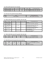
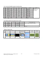
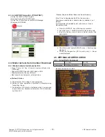
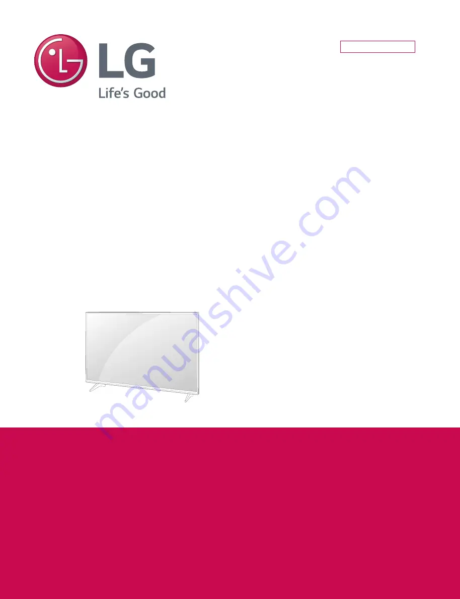
background image

CHASSIS : 6L60N

MODEL : 50UH5500

CAUTION

BEFORE SERVICING THE CHASSIS,

READ THE SAFETY PRECAUTIONS IN THIS MANUAL.

LED TV

SERVICE MANUAL

Internal Use Only

Summary of Contents for 50UH5500 65UH5500

Page 1: ...CHASSIS 6L60N MODEL 50UH5500 CAUTION BEFORE SERVICING THE CHASSIS READ THE SAFETY PRECAUTIONS IN THIS MANUAL LED TV SERVICE MANUAL Internal Use Only ...

Page 2: ...served Only for training and service purposes CONTENTS CONTENTS 2 SAFETY PRECAUTIONS 3 SERVICING PRECAUTIONS 4 SPECIFICATION 6 ADJUSTMENT INSTRUCTION 14 BLOCK DIAGRAM 26 EXPLODED VIEW 34 DISASSEMBLY 35 SCHEMATIC CIRCUIT DIAGRAM APPENDIX TROUBLE SHOOTING GUIDE APPENDIX ...

Page 3: ...inals etc to be sure the set is safe to operate without damage of electrical shock Leakage Current Cold Check Antenna Cold Check With the instrument AC plug removed from AC source connect an electrical jumper across the two AC plug prongs Place the AC switch in the on position connect one lead of ohm meter to the AC plug prongs tied together and touch other ohm meter lead in turn to each exposed m...

Page 4: ...lectrostatic charge on your body by touching a known earth ground Alter natively obtain and wear a commercially available discharging wrist strap device which should be removed to prevent poten tial shock reasons prior to applying power to the unit under test 2 After removing an electrical assembly equipped with ES devices place the assembly on a conductive surface such as aluminum foil to prevent...

Page 5: ...he solder joints of the two original leads If they are not shiny reheat them and if necessary apply additional solder Fuse and Conventional Resistor Removal Replacement 1 Clip each fuse or resistor lead at top of the circuit board hollow stake 2 Securely crimp the leads of replacement component around notch at stake top 3 Solder the connections CAUTION Maintain original spacing between the replace...

Page 6: ...rmance LGE TV test method followed 2 Demanded other specification Safety UL CSA CE IEC specification EMC FCC ICES CE IEC specification Wireless Wireless HD Specification Option No Item Specification Remark 1 Market North America 2 Broadcasting system ATSC NTSC M 64 256 QAM 3 Available Channel VHF 2 13 UHF 14 69 DTV 2 69 CATV 1 135 CADTV 1 135 4 Receiving system Digital ATSC 64 256 QAM Analog NTSC ...

Page 7: ...2 Aspect Ratio 16 9 All 4 Operating Environment TFT 1 Temp 0 40 deg 2 Humidity 0 85 LGE SPEC ALEF Temp 0 50 deg Humidity 20 90 5 Storage Environment TFT Temp 20 60 deg Humidity 10 90 ALEF Temp 20 60 deg Humidity 10 90 6 Input Voltage AC100 240V 50 60Hz 7 Display Colors 1 07 B 10 bit LGD 1 07G colors 8 bit FRC V580DJ2 KS5 1 067G V500DJ2 KS5 Surface Treatment Hard coating 2H Anti glare 4 2 Module Sp...

Page 8: ...72 59 94 74 176 HDTV 1080I 9 1920 1080 67 500 60 148 50 HDTV 1080P 10 1920 1080 67 432 59 94 148 352 HDTV 1080P No Resolution H freq kHz V freq kHz Pixel clock MHz Proposed HDMI PC DDC 1 640 350 31 46 70 09 25 17 EGA Х 2 720 400 31 46 70 08 28 32 DOS O 3 640 480 31 46 59 94 25 17 VESA VGA O 4 800 600 37 87 60 31 40 00 VESA SVGA O 5 1024 768 48 36 60 00 65 00 VESA XGA O 6 1152 864 54 34 60 05 80 00...

Page 9: ...0 27 00 24 00 74 25 HDTV 1080P 12 1920 1080 26 97 23 97 74 176 HDTV 1080P 13 1920 1080 33 75 30 00 74 25 HDTV 1080P 14 1920 1080 33 71 29 97 74 176 HDTV 1080P 15 3840 2160 67 5 30 00 297 00 UDTV 2160P 16 3840 2160 61 43 29 97 296 703 UDTV 2160P 17 3840 2160 56 25 25 00 297 00 UDTV 2160P 18 3840 2160 54 0 24 00 297 00 UDTV 2160P 19 3840 2160 53 95 23 98 296 703 UDTV 2160P 20 3840 2160 135 59 94 594...

Page 10: ... 45 59 94 60 148 35 148 5 4 Side by side Full HDTV 720P 4 1920 1080 33 72 33 75 59 94 60 74 18 74 25 5 Top and Bottom Side by side half Secondary HDTV 1080I Primary HDTV 1080I 67 43 67 5 59 94 60 148 35 148 5 5 Frame packing Field alternative Primary HDTV 1080I HDTV 1080I 33 72 33 75 59 94 60 148 35 148 5 5 Side by side Full HDTV 1080I 26 97 27 23 97 24 74 18 74 25 32 Top and Bottom Side by side h...

Page 11: ...2160 56 25 25 00 297 00 HDTV 2160P 11 3840 2160 61 43 29 970 296 703 HDTV 2160P 12 3840 2160 67 5 30 00 297 00 HDTV 2160P 13 4096 2160 53 95 23 976 296 703 HDTV 2160P 14 4096 2160 54 24 00 297 00 HDTV 2160P 15 4096 2160 56 25 25 00 297 00 HDTV 2160P 16 4096 2160 61 43 29 970 296 703 HDTV 2160P 17 4096 2160 67 5 30 00 297 00 HDTV 2160P 18 3840 2160 135 60 594 HDTV 2160P 2D to 3D Top Bottom half Sid...

Page 12: ...tible Side by Side Half Top Bottom No Resolution H freq kHz V freq Hz Pixel clock MHz 3D input proposed mode 1 Under 704x480 2D to 3D 2 Over 704x480 interlaced 2D to 3D Side by Side Half Top Bottom 3 Over 704x480 progressive 60 2D to 3D Side by Side Half Top Bottom Checker Board Row Interleaving Column Interleaving Frame Sequential 4 Over 704x480 progressive others 2D to 3D Side by Side Half Top B...

Page 13: ...MHz Proposed Remark 1 1280 720 45 00 60 00 74 25 HDTV 720P 2D to 3D Side by Side Half Top Bottom 2 1280 720 37 500 50 74 25 HDTV 720P 3 1920 1080 33 75 60 00 74 25 HDTV 1080I 4 1920 1080 28 125 50 00 74 25 HDTV 1080I 5 1920 1080 27 00 24 00 74 25 HDTV 1080P 6 1920 1080 28 12 25 74 25 HDTV 1080P 7 1920 1080 33 75 30 00 74 25 HDTV 1080P 8 1920 1080 67 50 60 00 148 5 HDTV 1080P 9 1920 1080 56 250 50 ...

Page 14: ... be also performed in Final Assembly if needed Both Board level and Final assembly adjustment items can be check using In Start Menu 1 ADJUST CHECK 3 2 Final assembly adjustment White Balance adjustment RS 232C functionality check PING Test Factory Option setting per destination Ship out mode setting In Stop 3 3 Etc Ship out mode Service Option Default USB Download S W Update Option Service only I...

Page 15: ... Widevine 4 Play START 5 Check of result Ready Test OK or NG 4 2 4 Communication Port connection 1 Connect PCBA Jig RS 232C Port PC RS 232C Port 4 2 5 Download 1 Models MAC Widevine ESN Korea model K2Lp 4 3 LAN Inspection 4 3 1 Equipment Condition Each other connection to LAN Port of IP Hub and Jig 4 3 2 LAN inspection solution LAN Port connection with PCB Network setting at MENU Mode of TV Settin...

Page 16: ...erated by Manufacturing Technology Group C Serial number D L must be conformed when it is produced in production line because serial number D L is mandatory by D book 4 0 Manual Download Model Name and Serial Number If the TV set is downloaded By OTA or Service man Sometimes model name or serial number is initialized not always It is impossible to download by bar code scan so It need Manual downlo...

Page 17: ...0x01 ཱྀ 01 03 80 A0 5A 78 0A EE 91 A3 54 4C 99 26 0x02 0F 50 54 A1 8 00 31 40 45 40 61 40 71 40 81 80 0x03 01 01 01 01 01 01 02 3A 80 18 71 38 2D 40 58 2C 0x04 45 00 40 84 63 00 00 1E 66 21 50 B0 51 00 1B 30 0x05 40 70 36 00 40 84 63 00 00 1E 00 00 00 FD 00 3A 0x06 3E 1E 53 10 00 0A 20 20 20 20 20 20 0x07 01 ᐗ1 0x00 02 03 3A F1 4E 10 9F 04 13 05 14 03 02 12 20 21 0x01 22 15 01 29 3D 06 C0 15 07 50 ...

Page 18: ... FF FF FF FF FF FF 00 1E 6D 01 00 01 01 01 01 10 01 1A 01 03 80 A0 5A 78 0A EE 91 A3 54 4C 99 26 20 0F 50 54 A1 08 00 31 40 45 40 61 40 71 40 81 80 30 01 01 01 01 01 01 08 E8 00 30 F2 70 5A 80 B0 58 40 8A 00 40 84 63 00 00 1E 02 3A 80 18 71 38 2D 40 50 58 2C 45 00 40 84 63 00 00 1E 00 00 00 FD 00 3A 60 3E 1E 88 3C 00 0A 20 20 20 20 20 20 00 00 00 FC 70 00 4C 47 20 54 56 0A 20 20 20 20 20 20 20 01 ...

Page 19: ...0 80 01 02 03 04 E3 0E 61 66 E3 30 06 07 01 01 1D 80 18 71 1C 16 20 58 2C 25 00 40 40 84 63 00 00 9E 66 21 50 B0 51 00 1B 30 40 70 36 50 00 40 84 63 00 00 1E 00 00 00 00 00 00 00 00 00 60 00 00 00 00 00 00 00 00 00 00 00 00 00 00 00 00 70 00 00 00 00 00 00 00 00 00 00 00 00 00 00 00 0A 0 1 2 3 4 5 6 7 8 9 A B C D E F 0 FF FF FF FF FF FF 00 1E 6D 01 00 01 01 01 01 01 10 1A 01 03 80 A0 5A 78 0A EE 9...

Page 20: ... A B C D E F 0 00 FF FF FF FF FF FF 00 1E 6D 01 00 01 01 01 01 10 01 1A 01 03 80 A0 5A 78 0A EE 91 A3 54 4C 99 26 20 0F 50 54 A1 08 00 31 40 45 40 61 40 71 40 81 80 30 01 01 01 01 01 01 08 E8 00 30 F2 70 5A 80 B0 58 40 8A 00 40 84 63 00 00 1E 02 3A 80 18 71 38 2D 40 50 58 2C 45 00 40 84 63 00 00 1E 00 00 00 FD 00 3A 60 3E 1E 88 3C 00 0A 20 20 20 20 20 20 00 00 00 FC 70 00 4C 47 20 54 56 0A 20 20 2...

Page 21: ...ED Module CH 14 or CM H505 2 Adj Computer During auto adj RS 232C protocol is needed 3 Adjust Remocon 4 Signal internal flicker Pattern in SET Color Analyzer Matrix should be calibrated using CS 100 5 4 3 Equipment connection MAP 5 4 4 Adj Command Protocol Command Format CMD ID DATA CR RF CMD Command ID Command Data Command Ex Send va 00 00 r n 1 RS 232C Command used during auto adj RS 232C COMMAN...

Page 22: ...0 Begin White Balance adj wb 00 10 Gain adj internal white pattern wb 00 1f Gain adj completed wb 00 20 Offset adj internal white pattern wb 00 2f Offset adj completed wb 00 ff End White Balance adj internal pattern disappears Ex wb 00 00 Begin white balance auto adj wb 00 10 Gain adj ja 00 ff Adj data jb 00 c0 wb 00 1f Gain adj complete wb 00 20 start wb 00 2f endc Off set adj wb 00 ff End white ...

Page 23: ...N status during 5 Minutes In case of LCD Back light on should be checked using no signal or Full white pattern 5 5 6 Reference White Balance Adj coordinate and color temperature Luminance 206 Gray Standard color coordinate and temperature using CS 1000 over 26 inch Mode Coordinate Temp uv X Y Cool 0 271 0 270 13 000K 0 0000 Medium 0 283 0 289 9 300K 0 0000 Warm 0 313 0 329 6 500K 0 0000 Standard c...

Page 24: ...es Check the picture like below 5 9 HDMI ARC Function Inspection 5 9 1 Test equipment Optic Receiver Speaker MSHG 600 SW 1220 HDMI Cable for 1 4 version 5 9 2 Test method 1 Insert the HDMI Cable to the HDMI ARC port from the master equipment HDMI2 2 Check the sound from the TV Set 3 Check the Sound from the Speaker or using AV Optic TEST program It s connected to MSHG 600 5 10 EYE Q Green Function...

Page 25: ... Item Min Typ Max Unit Remark 1 Audio practical max Output L R Distortion 10 max Output 10 0 8 10 12 0 10 8 W Vrms EQ Off AVL Off Clear Voice Off 2 Speaker 8Ω Impedance 10 12 W EQ On AVL On Clear Voice On Measurement condition 1 RF input Mono 1KHz sine wave signal 100 Modulation 2 CVBS Component 1KHz sine wave signal 0 4Vrms 3 RGB PC 1KHz sine wave signal 0 7Vrms 8 USB S W Download optional Servic...

Page 26: ...al eMMC 4GB CI Slot OCP USB1 2 0 HDMI3 ARC HDMI2 HDMI1 Air Cable TUNER T2 C A TUNER S2 DVB S DEMOD S2 LNB T2 C S2 W O AD REAR H IF P_TS P_TS_OUT P_TS_IN Sub Micom RENESAS R5F100GEAFB X_TAL 32 768KHz I2C_MICOM HW Port IR KEY WIFI 11n only USB_WIFI X_TAL 24MHz Sub Assy LAN ETHERNET OPTIC AV COMP CVBS YPbPr SPDIF OUT RS 232 MAX323 MAIN Audio AMP NTP7515 I2S Out I2C 4 Vx1 51P 8 lane Vx1 I2C 6 M0 M1 P_...

Page 27: ...2C_SCL Realtek K2Lp 33 34 B 2 HSYNC 1 8k Ω 3 3V_NOR 1 8k Ω 1 8k Ω 3 3V_NOR IC3000 R5F100GEAFB MICOM 1 2 H2 GPIO_T_SCL H1 GPIO_T_SDA I2C_SDA4 I2C_SCL4 IC101 NVRAM IC5800 NTP7515 AMP E13 ST_IO03 F13 ST_IO02 I2C_SDA2 I2C_SCL2 IC6901 A8303SESTR T LNB TU6701 TDJM G301D 27 SCL_DEMOD 30 SDA_DEMOD 7 8 1 8 k Ω 1 8 k Ω 3 3V_TU 4 SCL_RF 5 SDA_RF 1 8k Ω 1 8k Ω 3 3V_NOR 33 Ω TCON_I2C_EN 33 Ω 33 Ω 33 Ω 100Ω 33 ...

Page 28: ...231 IC2300 1 0V ETH ST LDO 1A SoC K2L 3 5V ST BY 4A TI TPS56428 IC2306 0 75A 0 18A 0 51A 0 98A 0 41A 0 7A 5V Normal 6A Rohm RT7231 IC2500 WIFI Panel LNB EU option MICOM IR ETC 0 1A 1A 0 17A SOC 0 02A 1 97A 5 68A 1 2V Tuner 2A TJ2132 0 6A 1 8V eMMC 2A 0 2A 1 41A 2 47A 0 5A 5 6 1 0V_CORE DC DC 10A TI TPS51362 IC2305 1 5V DDR DC DC 3A BD9A300 IC2303 1A 3 3V Normal 2A TJ2132 IC2301 TUNER 0 4A ...

Page 29: ...POD0 TPDO7 2 5V_DEMOD 38 2 5V_Normal TU_RESET1_TU 25 TU_RESET1 AN6 GPIO14_DIGI_MIC 3 3V_LNA_TU 1 LNB_TX1 29 LNB_OUT1 31 I2C_SCL2_TU 27 I2C_SDA2_TU 30 I2C_SCL2 I2C_SDA2 3 3V_TU 3 3V_NORMAL IF_P IF_N TUNER_SIF TU_CVBS IF_AGC AT2 IF_P AT3 IF_N AG1 VIN10P AM6 GPIO0_RF_IF_AGC1 I2C_SCL5_TU 4 I2C_SDA5_TU 5 D_DEMOD_CORE LNB1 IC6901 A8303SESTR TB LNB_TX1 LNB_OUT1 1 8K Ω 7 SCL 8 SDA 10 TONECTRL 2 LNB 33 Ω F...

Page 30: ...poses 5 Video Audio In Block Diagram Realtek K2Lp COMP1_Y CVBS VIN4P E2 Jack Side SOC Side SPDIF_OUT SPDIF OUT H P JACK HP_L ROUT_AMP SPDIF_OUT C5 HPOL R F4 F5 HP_L ROUT AMP IC6100 VIN3P D2 VIN5P E3 AI1L A4 COMP1_Pb COMP1_Pr AI1R B4 COMP1 AV1 DVI_L_IN COMP1 AV1 DVI_R_IN US Model use this jack for SVC RS 232C ...

Page 31: ...PIO90_SCLK AM27 GPIO89_WCLK AK28 GPIO93_MCLK AL27 HPOL F4 HPOR F5 TU_SIF GPIO1_T_SCL H2 GPIO2_T_SDA H1 H P AMP TPA6138A2 IC6100 LPF AI2R SPDIF_OUT COMP1 AV1 DVI_L R_IN A4 AI1L B4 AI1R HP_L ROUT_AMP LPF LPF Realtek K2Lp Tuner D11 SPDIF_OUT AUD_LRCH AUD_LRCK AMP_MUTE SPK_R R SPK_L L MAIN AMP NTP7515 IC5800 MICOM SPK L SPK R 22 27 38 CLK_I 8 WCK 7 AUD_LRCH 10 11 36 30 33 18 21 AV COMP HDMI3 SPDIF US ...

Page 32: ...ST_IO22_H1_SCL C6 ST_IO23_H1_SDA B6 CEC_REMOTE P0 TMDS1 D0 D1 D2 CLK ST_IO25_H2_SCL G5 ST_IO26_H2_SDA E6 DDC_SCL1 DDC_SDA1 DDC 5V PULL UP 47kΩ DDC 5V PULL UP 47 k Ω MICOM R5F100GEAFB IC3000 P2 TMDS3 D0 D1 D2 CLK HDMI_HPD_3 DDC_SCL3 DDC_SDA3 ST_IO21_H0_HPD A7 ST_IO19_H0_SCL C7 ST_IO20_H0_SDA B7 EEPROM BR24G02 IC3301 DDC 5V PULL UP 47 k Ω 22 Ω CEC_REMOTE CEC_REMOTE HDMI_HPD_3 HDMI_ARC KOREA Model on...

Page 33: ...ghts reserved Only for training and service purposes 8 USB WIFI UART 3 5V_ST Switch IC 3 5V_WOL 3 5V_ST Switch IC 3 5V_WIFI K2Lp MICOM POWER ON WIFI_DP DM WiFi TDP TDN RDP RDN LAN WOL_CTRL 3 5V_WIFI WOL ETH_POWER_ON WOL WIFI_POWER_ON 3 5V_ST WIFI_EN IC4102 IC5201 ...

Page 34: ...characteristics These parts are identified by in the Schematic Diagram and EXPLODED VIEW It is essential that these special safety parts should be replaced with the same components as recommended in this manual to prevent Shock Fire or other Hazards Do not modify the original design without permission of manufacturer IMPORTANT SAFETY NOTICE 900 540 400 521 500 522 530 570 200 600 120 121 700 A10 S...

Page 35: ...ifying locations can be inserted below 1 Unlock screw A 17EA and B 4EA to separate back cover assembly Unlock screw C 4EA to separate the base Fig 1 2 Separate the cushion D E from backcover Fig 2 3 Unlock screw F 5EA to sepparate power board Unlock screw F 4EA to sepparate main board and AV bracket G H Unlock screw F 8EA to sepparate wall mounting bracket Fig 3 5 Unlock screw A 1EA to separate wi...

Page 36: ... 36 LGE Internal Use Only Copyright LG Electronics Inc All rights reserved Only for training and service purposes Fig 1 A A A A B A A A A B C C C C A A A A A A B B A A A Fig 2 E E E D ...

Page 37: ... 37 LGE Internal Use Only Copyright LG Electronics Inc All rights reserved Only for training and service purposes Fig 3 F F F F G H F F F F F F F F F F F F F Fig 4 I ...

Page 38: ... 38 LGE Internal Use Only Copyright LG Electronics Inc All rights reserved Only for training and service purposes Fig 5 J A ...

Page 39: ..._H0_HPD A7 ST_IO19_H0_SCL C7 ST_IO20_H0_SDA B7 ST_IO24_H1_HPD F6 ST_IO22_H1_SCL C6 ST_IO23_H1_SDA B6 ST_IO25_H2_SCL G5 ST_IO26_H2_SDA E6 ST_IO27_VGA_SCL B3 ST_IO28_VGA_SDA A3 RTC_XI A10 RTC_XO B10 RST A9 ST_IO02 F13 ST_IO03 E13 ST_IO04 F12 ST_IO05 E12 ST_IO06 F11 ST_IO07 E11 ST_IO08 D11 ST_IO09 F10 ST_IO10 E10 ST_IO11 F9 ST_IO12 E9 ST_IO13 D9 ST_IO14 F8 ST_IO15 E8 ST_IO16 F7 ST_IO17 E7 ST_IO18 D7 ...

Page 40: ...L208 BLM18PG121SN1D C213 0 1uF DDR_CS_ON_OFF C219 0 1uF 1 5V_DDR C249 10uF 10V C217 0 1uF C246 10uF 10V 3 5V_WOL R212 100 L201 BLM18PG121SN1D R209 5 1K C220 0 1uF C210 0 1uF 16V C238 10uF 10V L207 BLM18PG121SN1D Q204 SSM3J332R S G D C223 0 1uF 3 5V_ST R204 10K C231 10uF 10V IC200 AP7361 Y 13 3 ADJ NC 2 GND 4 IN 1 EN 5 OUT ZD200 2 5V C241 10uF 10V WOL_CTL R206 20K 1 ST_A1V0 R205 5 1K 1 IC100 LGE655...

Page 41: ...DQ_7 F1 VDDQ_8 H2 VDDQ_9 H9 NC_1 J1 NC_2 J9 NC_3 L1 NC_4 L9 A14 T7 VSS_1 A9 VSS_2 B3 VSS_3 E1 VSS_4 G8 VSS_5 J2 VSS_6 J8 VSS_7 M1 VSS_8 M9 VSS_9 P1 VSS_10 P9 VSS_11 T1 VSS_12 T9 VSSQ_1 B1 VSSQ_2 B9 VSSQ_3 D1 VSSQ_4 D8 VSSQ_5 E2 VSSQ_6 E8 VSSQ_7 F9 VSSQ_8 G1 VSSQ_9 G9 M0_DDR_DQ12 M0_DDR_BA2 M0_DDR_DQ27 M0_DDR_A11 M0_DDR_DQ10 1 5V_DDR M0_DDR_DQ4 M0_DDR_DQ28 C428 0 1uF 16V M0_DDR_A3 C402 0 1uF 16V M0...

Page 42: ...AP3_L TXDAN1_L TXDAP1_L TXDAP0_L TXDAN0_L VX1_MSE AGP_CTRL IC100 LGE6551 CA1 LVDS_AAN B25 LVDS_AAP A25 LVDS_ABN B24 LVDS_ABP A24 LVDS_ACN B23 LVDS_ACP A23 LVDS_ADN B22 LVDS_ADP A22 LVDS_AEN B21 LVDS_AEP A21 LVDS_AFN B20 LVDS_AFP A20 LVDS_BAN AF28 LVDS_BAP AF27 LVDS_BBN AG28 LVDS_BBP AG27 LVDS_BCN AH28 LVDS_BCP AH27 LVDS_BDN AJ28 LVDS_BDP AJ27 LVDS_BEN B27 LVDS_BEP A27 LVDS_BFN B26 LVDS_BFP A26 LVD...

Page 43: ...28 DGND_86 W3 DGND_87 W4 DGND_88 W5 DGND_89 W9 DGND_90 W15 DGND_91 W16 DGND_92 W17 DGND_93 W18 DGND_94 W19 DGND_95 W20 DGND_96 W21 DGND_97 W22 DGND_98 W23 DGND_99 W26 DGND_100 W29 DGND_101 W31 DGND_102 Y3 DGND_103 Y4 DGND_104 Y5 DGND_105 Y15 DGND_106 Y16 DGND_107 Y17 DGND_108 Y18 DGND_109 Y19 DGND_110 Y20 DGND_111 Y21 DGND_112 Y22 DGND_113 Y23 DGND_114 Y26 DGND_115 AA4 DGND_116 AA15 DGND_117 AA16 ...

Page 44: ...16W CI_SLOT TPI_DATA 0 TPI_DATA_CI 3 TPI_DATA_CI 0 EB_DATA 2 CI_DATA 4 TPI_VAL_CI CAM_REG_N R912 100 CI_SLOT CI_OE CI_ADDR 3 C903 0 1uF CI_SLOT TPI_DATA 6 EB_OE_N TPI_DATA 1 AR901 33 1 16W CI_SLOT R909 10K CI_SLOT TPI_DATA_CI 2 TPI_DATA_CI 2 EB_DATA 3 AR903 33 1 16W CI_SLOT TPI_SOP_CI CI_ADDR 14 C904 0 1uF CI_SLOT TPI_DATA 4 CAM_IREQ_N CI_MDI 4 R922 100 CI_SLOT 5V_NORMAL TPI_DATA 2 R910 100 CI_SLO...

Page 45: ...1K R2331 14K 1 PD_ 12V 13V Q2302 1 2N7002KA FET_KEC G D S 3 3V_NORMAL C2316 4700pF 50V C2351 10uF 25V C2301 10uF 10V R2332 5 1K 1 PD_ 12V 3 3V_NORMAL C2343 470pF 50V OPT C2354 10uF 10V R2338 0 1 16W 5 R2321 4 7 5 C2304 10uF 10V R2333 0 5 PD_ 3 5V R2307 10K R2340 240K 1 16W 1 R2313 0 5 C2308 0 1uF 16V C2335 0 1uF 16V OPT C2347 0 01uF 25V C2303 10uF 10V C2356 0 1uF 16V NON_OLED ZD2304 2 5V R2300 6 8...

Page 46: ...16V OPT C2500 0 1uF 16V OPT R2519 36K VA2500 ADUC 20S 02 010L OPT R2517 10K A13V L D_CLK R2507 100 55INCH_BOE_M _MODULE C2511 10uF 25V 3 3V_NORMAL C2513 10uF 10V R2521 3 3K LVDS_DISCHARGE Q2503 MMBT3904 NXP E B C C2508 10uF 25V P2502 SMAW200 H12S5K BK LTR PSU_12P ZD2500 5V 13V C2524 10uF 25V C2522 0 1uF 50V R2503 100 PSU_MODE_SELECT_NON INV_CTL C2512 10uF 25V MODE_SELECT R2511 10K C2501 1uF 10V 4 ...

Page 47: ...1 P70 KR0 SCK21 SCL21 12 P30 INTP3 RTC1HZ SCK11 SCL11 13 P50 INTP1 SI11 SDA11 14 P51 INTP2 SO11 15 P17 TI02 TO02 16 P16 TI01 TO01 INTP5 17 P15 PCLBUZ1 SCK20 SCL20 18 P14 RXD2 SI20 SDA20 19 P13 TXD2 SO20 20 P12 SO00 TXD0 TOOLTXD 21 P11 SI00 RXD0 TOOLRXD SDA00 22 P10 SCK00 SCL00 23 P146 24 P147 ANI18 25 P27 ANI7 26 P26 ANI6 27 P25 ANI5 28 P24 ANI4 29 P23 ANI3 30 P22 ANI2 31 P21 ANI1 AVREFM 32 P20 AN...

Page 48: ...M_LOGO OLED R3009 3 20K MICOM_UHD R3009 4 75K MICOM_8K R3009 1 2 7K MICOM_FHD R3011 2 8 2K MICOM_RTK R3011 4 75K MICOM_M2 R3011 1 2 7K MICOM_M16 R3011 3 20K MICOM_H15 A5LR NON LOGO LCD MODEL_OPT_0 AM0 MICOM MODEL OPTION LOGO LCD 0 72V MODEL_OPT_2 AM2 1 53V BOX_NON_EPI TV_NON_EPI FHD MODEL_OPT_3 AM3 UHD M16 MODEL_OPT_1 AM1 H15 2 27V 3 0V NON LOGO OLED LOGO OLED MODEL_OPT_3 AM3 TV_EPI BOX_NON_EPI 8K...

Page 49: ...TECH_2 VA3311 1 ADMC 5M 02 200L EAF61530101 ESD_HDMI_AMOTECH_2 VA3314 1 ADMC 5M 02 200L EAF61530101 ESD_HDMI_AMOTECH_2 VA3301 1 ADUC 20S 02 010L EAF61530301 ESD_HDMI_AMOTECH_2 VA3302 1 ADUC 20S 02 010L EAF61530301 ESD_HDMI_AMOTECH_2 VA3304 1 ADUC 20S 02 010L EAF61530301 ESD_HDMI_AMOTECH_2 VA3305 1 ADUC 20S 02 010L EAF61530301 ESD_HDMI_AMOTECH_2 VA3306 1 ADUC 20S 02 010L EAF61530301 ESD_HDMI_AMOTEC...

Page 50: ... C3816 0 22uF 25V HP_OUT C3802 560pF 50V OPT C3805 27pF 50V OPT COMP1_DET R3817 75 1 R3832 0 R3811 0 R3802 1K DTV MNT_V_OUT R3816 75 1 JK3801 PEJ034 01 JACK_HP_OUT RS232C EAG60841811 6B T_TERMINAL2 7B B_TERMINAL2 5 T_SPRING 4 R_SPRING 3 E_SPRING L3800 BLM18PG121SN1D HP_OUT VA3803 5 6V R3803 1K R3808 75 1 4W 1 C3820 390pF 50V OPT COMP1 AV1 DVI_L_IN COMP1_Y CVBS R3819 1 22uF 16V HP_AMP_NON HP_ROUT_A...

Page 51: ...4100 0 1uF AR4101 100 1 16W WIFI_DP C4105 100pF 50V C4102 0 1uF 16V OPT M_RFModule_RESET WIFI_EN 3 5V_WIFI C4107 5pF 50V OPT LED_R C4112 0 1uF OPT R4101 33 R4117 2K OPT D4100 WIFI_DIODE_TOSHIBA EAH62735601 D4100 1 WIFI_DIODE_SEMTECH EAH61515101 R4118 0 1 16W 5 OPT R4119 0 1 16W WIFI_11N_ONLY P4100 12507WR H21L2B BK 1 VCC 2 USB D 3 USB D 4 GND 5 WL_HOST_WAKE 6 GND 7 BT_REG_ON 8 GND 12 SDA 13 SCL 14...

Page 52: ...REAR C4322 10uF 10V USB_REAR R4301 10K USB_REAR USB_CTL1 USB_DP1 5V_NORMAL R4303 4 7K USB_REAR JP4300 JP BLOCK USB VBUS DM DP GND 5V_USB_1 5V_USB_1 3 3V_NORMAL C4323 10uF 10V USB_REAR USB_DM1 D4301 5V USB_REAR_ESD_DIODE D4302 DF3D6 8MS USB_REAR R4309 2 2 USB_REAR R4308 2 2 USB_REAR IC4301 BD2242G USB_REAR EAN62871401 3 EN 2 GND 4 OC 1 VIN 6 VOUT 5 ILIM R4305 14K 1 USB_REAR USB1 OCP USB2_2 0 MAX 1 ...

Page 53: ...02 0 1uF 16V USB_SIDE USB3_DM0 USB3_DP0 USB3_TXM0 USB3_TXP0 ZD4400 5V USB_SIDE_ESD_DIODE M4400 JP BLOCK USB VBUS DM DP GND 5V_USB_2 D4400 DF3D6 8MS USB_SIDE C4400 10uF 10V JK4400 3AU04S 305 ZC LG USB_SIDE 1 2 3 4 5 C4401 10uF 10V USB3_RXM0 USB3_RXP0 USB_OCD1 USB_CTL1 USB_DM1 USB_DP1 R4401 2 2 USB_SIDE R4400 2 2 USB_SIDE IC4400 BD2242G USB_SIDE 3 EN 2 GND 4 OC 1 VIN 6 VOUT 5 ILIM R4404 14K 1 USB_SI...

Page 54: ...5000 0 OPT C5000 0 1uF 16V NON_EASY_TV EPHY_TDN EPHY_RDN R5001 0 OPT VA5001 5 5V NON_EASY_TV VA5002 5 5V NON_EASY_TV EPHY_TDP C5001 0 01uF 50V NON_EASY_TV L5000 PZ1608U121 2R0TF NON_EASY_TV JK5000 RJ45VT 01SN002 LANJACK_UDE_MAIN EAG35781010 1 1 2 2 3 3 4 4 5 5 6 6 7 7 8 8 9 9 JK5000 1 26TM9G 30100 02HF LANJACK_FREEPORT_SUB1 EAG35781016 1 1 2 2 3 3 4 4 5 5 6 6 7 7 8 8 9 9 JK5000 2 B50 512 10 F4 03A...

Page 55: ...DD1B 32 PVDD1A 33 OUT1A 34 PGND1A 35 BST1A 36 RESET 37 AD 38 CLK_I 39 GND_IO 40 VDD_IO 41 EP GND C5813 390pF 50V 0 1uF C5805 16V R5800 10K I2C_SCL4 C5812 22000pF 50V TP5801 0 1uF C5822 50V AR5800 100 13V_AMP C5819 0 47uF 50V WOOFER_MUTE C5806 1000pF 50V AMP_RESET_N R5809 3 3 1 10W 5 R5813 4 7K R5814 4 7K WOOFER_MUTE L5803 10 0uH NRS6045T100MMGK I2C_SDA4 C5811 22000pF 50V TP5802 R5808 3 3 1 10W 5 L...

Page 56: ... 0 1uF 16V HP_AMP R6103 43K 1 HP_AMP R6102 43K 1 HP_AMP C6103 1uF 10V HP_AMP R6107 0 HP_AMP_NON SIDE_HP_MUTE HP_ROUT_AMP C6111 0 01uF OPT C6104 18pF HP_AMP 3 3V_NORMAL C6105 1uF 10V HP_AMP IC6100 TPA6138A2 HP_AMP 3 OUTR 2 INR 4 GND_1 1 INR 6 VSS 5 MUTE 7 CN 8 CP 9 VDD 10 GND_2 11 UVP 12 OUTL 13 INL 14 INL HP_LOUT_AMP C6108 10pF 50V HP_AMP C6106 10pF 50V HP_AMP C6100 2 2uF 10V HP_AMP C6109 18pF HP_...

Page 57: ...TU_ALL LNB_OUT 3 3V_NORMAL R6504 0 TU_ALL_IntDemod IF_N_TU R6500 10K TU_N D C6511 0 1uF TU_N D L6502 OPT TU_SIF_TU L6503 PZ1608U121 2R0TF TU_N D 3 3V_NORMAL FE_DEMOD1_TS_SYNC FE_DEMOD1_TS_VAL FE_DEMOD1_TS_DATA 2 FE_DEMOD1_TS_DATA 4 FE_DEMOD1_TS_DATA 0 7 FE_DEMOD1_TS_DATA 1 FE_DEMOD1_TS_DATA 3 FE_DEMOD1_TS_DATA 6 FE_DEMOD1_TS_DATA 7 FE_DEMOD1_TS_DATA 5 FE_DEMOD1_TS_DATA 0 C6512 0 1uF OPT IF_P_MAIN ...

Page 58: ...YNC 17 VALID 18 DATA0 19 DATA1 20 DATA2 21 DATA3 22 DATA4 23 DATA5 24 DATA6 25 DATA7 26 LNB 27 GND_2 28 SHIELD TU6701 2 TDJN K301F TU_N_CO 1 SCL_RF 2 SDA_RF 3 B1 3 3V 4 CVBS 5 AIF_AGC 6 SIF 7 AIF N 8 AIF P 9 GND_1 10 RESET_DEMOD 11 B2 3 3V 12 F22_OUTPUT 13 B3 1 2V 14 ERROR 15 MCLK 16 SYNC 17 VALID 18 DATA0 19 DATA1 20 DATA2 21 DATA3 22 DATA4 23 DATA5 24 DATA6 25 DATA7 26 LNB 27 GND_2 28 SHIELD TDJ...

Page 59: ...10K 1 16W 5 LNB C6910 0 1uF 50V LNB R6910 36K LNB C6906 10uF 25V LNB A_GND 3 3V_NORMAL A_GND R6904 0 R6905 0 LNB_Tx C6904 0 1uF 50V LNB R6911 150K LNB A_GND LNB_TX C6902 0 22uF 25V LNB C6913 0 1uF 50V LNB C6908 0 1uF LNB C6900 0 1uF LNB A_GND AR6900 33 LNB D6904 40V LNB SX34 D6903 40V LNB SX34 13V_M R6902 10K LNB_JAPAN R6902 1 0 NON_JAPAN_LNB R6901 27K LNB_JAPAN Q6900 MMBT3904 NXP LNB EBK61012601 ...

Page 60: ...F LGD BOE_PANEL_VX1 C7108 0 1uF LGD BOE_PANEL_VX1 C7112 0 1uF LGD BOE_PANEL_VX1 C7113 0 1uF LGD BOE_PANEL_VX1 C7110 0 1uF LGD BOE_PANEL_VX1 C7115 0 1uF LGD BOE_PANEL_VX1 C7114 0 1uF LGD BOE_PANEL_VX1 C7117 0 1uF LGD BOE_PANEL_VX1 C7116 0 1uF LGD BOE_PANEL_VX1 PWM_TCON_OUT 3 3V_NORMAL HTPDAn_IN 3 3V_NORMAL HTPDAn R7126 0 OPT LOCKAn_IN LOCKAn R7113 0 LGD BOE_PANEL_VX1 R7114 0 LGD BOE_PANEL_VX1 R7117...

Page 61: ..._76 L13 NC_77 L14 NC_78 M1 NC_79 M2 NC_80 M3 NC_81 M7 NC_82 M8 NC_83 M9 NC_84 M10 NC_85 M11 NC_86 M12 NC_87 M13 NC_88 M14 NC_89 N1 NC_90 N3 NC_91 N6 NC_92 N7 NC_93 N8 NC_94 N9 NC_95 N10 NC_96 N11 NC_97 N12 NC_98 N13 NC_99 N14 NC_100 P1 NC_101 P2 NC_102 P8 NC_103 P9 NC_104 P11 NC_105 P12 NC_106 P13 NC_107 P14 DAT7 EMMC_VDDI AR8100 0 1 16W DVDD18_EMMC EMMC_RESET_BALL EMMC_CLK EMMC_DATA 3 EMMC_RST AR...

Page 62: ... 7500 C11200 0 1uF RS232C C11202 0 1uF RS232C 3 5V_ST C11201 0 1uF RS232C SOC_RX RIN1 SOC_TX IC11200 MAX3232CDR EAN41348201 RS232C 3 C1 2 V 4 C2 1 C1 6 V 5 C2 7 DOUT2 8 RIN2 9 ROUT2 10 DIN2 11 DIN1 12 ROUT1 13 RIN1 14 DOUT1 15 GND 16 VCC AR11200 100 1 16W RS232C C11203 0 1uF RS232C DOUT1 C11204 0 1uF RS232C VA11200 OPT EAF61630102 VA11201 OPT EAF61630102 RS 232C Control INTERFACE Closed to Jack si...

Page 63: ......

Page 64: ...TROUBLE SHOOTING GUIDE Copyright 2016 LG Electronics Inc All rights reserved Only for training and service purposes LGE Internal Use Only ...

Page 65: ...f 7 8 C Audio error No audio Normal video 8 9 Wrecked audio discontinuation noise 9 10 D Function error Remote control Local switch checking 10 MR15 operating checking 11 Not used 11 Wifi operating checking 12 12 13 Camera operating checking 13 Not used 14 External device recognition error 14 15 E Noise Circuit noise mechanical noise 15 16 F Exterior error Exterior defect 16 First of all Check whe...

Page 66: ...Overview for 16 ULTRA HD Model K2Lp Hardware ...

Page 67: ...bps 4K 60Hz 4 2 2 10bit HDCP2 2 ARC MHL HDMI1 4 Legacy HDMI 3 O O O O X X O HDMI 2 O O O O O X O HDMI 1 O O O O X X O HDMI2 0 HDMI1 4 DVI All HDMI ports support ULTRA HD Deep Color If the device connected to Input Port also supports ULTRA HD Deep Color your picture may be Clearer ...

Page 68: ...LCD TV Repair Guide 16 years New Models Applicable Model UH55 ...

Page 69: ...Main PCB 210X183 UH55 From PSU Power T CON B D VX1 Audio Wifi Local Key IR 1 1 Main processor_ K2Lp DDR Memory eMMC Memory 2 3 Micom for Key IR sensing Audio AMP 3 2 ...

Page 70: ...iew Main External 1 K2Lp Block Diagram External 2 K2Lp Block Diagram Internal 3 K2Lp I2C Diagram 4 K2Lp Power Block Diagram 5 Tuner CI Block Diagram 6 Video Audio In Block Diagram 7 Audio Out Block Diagram 8 HDMI 9 USB WIFI UART 10 WOL TV Product Development Team 1 ...

Page 71: ...0 System Overview Main External 15 year UHD model 16 year UHD model ONLY 60HZ T120 Model 4K 60PX3EA K2Lp VX1 4K 60HZ 1 25GB ...

Page 72: ... 2 0 HDMI3 ARC HDMI2 HDMI1 Air Cable TUNER SIDE V IF P_TS_OUT P_TS_IN Sub Micom RENESA S R5F100GEAFB X_TAL 32 768KHz I2C_MICOM HW Port IR KEY WIFI 11n only USB_WIFI X_TAL 24MHz Sub Assy LAN ETHERNET OPTIC AV COMP CVBS YPbPr SPDIF OUT RS 232 MAX323 MAIN Audio AMP NTP7515 I2S Out I2C 4 Vx1 51P 8 lane Vx1 I2C 6 M0 M1 P_TS_IN IF NVRAM 256Kb I2C 4 I2C 2 EU ONLY ...

Page 73: ...2 K2Lp Block Diagram Internal LGE Confidential ...

Page 74: ... K2Lp 33 34 B 2 HSYNC 1 8k Ω 3 3V_NOR 1 8k Ω 1 8k Ω 3 3V_NOR IC3000 R5F100GEAFB MICOM 1 2 H2 GPIO_T_SCL H1 GPIO_T_SDA I2C_SDA4 I2C_SCL4 IC101 NVRAM IC5800 NTP7515 AMP E13 ST_IO03 F13 ST_IO02 I2C_SDA2 I2C_SCL2 TU6701 TDJS H351F 1 8 k Ω 1 8 k Ω 3 3V_TU 1 8k Ω 1 8k Ω 3 3V_NOR TCON_I2C_EN 33 Ω 33 Ω 100Ω LGE Confidential 33 Ω ...

Page 75: ...428 IC2306 0 75A 0 18A 0 51A 0 98A 0 41A 0 7A 5V Normal 6A Rohm RT7231 IC2500 WIFI Panel LNB EU option MICOM IR ETC 0 1A 1A 0 17A SOC 0 02A 1 97A 5 68A 1 2V Tuner 2A TJ2132 0 6A 1 8V eMMC 2A 0 2A 1 41A 2 47A 0 5A 1 0V_CORE DC DC 10A TI TPS51362 IC2305 1 5V DDR DC DC 3A BD9A300 IC2303 1A 3 3V Normal 2A TJ2132 IC2301 TUNER 0 4A LGE Confidential ...

Page 76: ...H351F K2Lp 3 3V_TUNER 11 IF_P_TU 6 IF_N_TU 7 TU_CVBS_TU 8 IF_AGC_TU 3 I2C_SCL2_TU 27 I2C_SDA2_TU 30 I2C_SCL2 I2C_SDA2 3 3V_TU 3 3V_NORMAL IF_P IF_N IF_AGC AT2 IF_P AT3 IF_N AG1 VIN10P AM6 GPIO0_RF_IF_AGC1 1 8K Ω AM5 GPIO1_T_SCL AM4 GPIO2_T_SDA 33 Ω ...

Page 77: ...P1_Y CVBS VIN4P E2 Jack Side SOC Side SPDIF_OUT SPDIF OUT H P JACK HP_L ROUT_AMP SPDIF_OUT C5 HPOL R F4 F5 HP_L ROUT AMP IC6100 VIN3P D2 VIN5P E3 AI1L A4 COMP1_Pb COMP1_Pr AI1R B4 COMP1 AV1 DVI_L_IN COMP1 AV1 DVI_R_IN US Model use this jack fo r SVC RS 232C ...

Page 78: ...AL27 HPOL F4 HPOR F5 TU_SIF GPIO1_T_SCL H2 GPIO2_T_SDA H1 H P AMP TPA6138A2 IC6100 LPF AI2R SPDIF_OUT COMP1 AV1 DVI_L R_IN A4 AI1L B4 AI1R HP_L ROUT_AMP LPF LPF K2Lp Tuner D11 SPDIF_OUT AUD_LRCH AUD_LRCK AMP_MUTE SPK_R R SPK_L L MAIN AMP NTP7515 IC5800 MICOM SPK L SPK R 22 27 38 CLK_I 8 WCK 7 AUD_LRCH 10 11 36 30 33 18 21 AV COMP HDMI3 SPDIF US Model use this jack fo r SVC RS 232C ...

Page 79: ...DS1 D0 D1 D2 CLK ST_IO25_H2_SCL G5 ST_IO26_H2_SDA E6 DDC_SCL1 DDC_SDA1 DDC 5V PULL UP 47kΩ DDC 5V PULL UP 47 kΩ MICOM R5F100GEAFB IC3000 P2 TMDS3 D0 D1 D2 CLK HDMI_HPD_3 DDC_SCL3 DDC_SDA3 ST_IO21_H0_HPD A7 ST_IO19_H0_SCL C7 ST_IO20_H0_SDA B7 EEPROM BR24G02 IC3301 DDC 5V PULL UP 47 kΩ 22 Ω CEC_Remote CEC_Remote HDMI_HPD_3 HDMI_ARC KOREA Model only support External EEPROM ...

Page 80: ... M_RFModule_RESET USB3_DM DP DEBUG_RX TX K2Lp HSDM1 AM3 HSDP1 AL3 HSDM3 A17 HSDP3 A18 USB1 MICOM R5F100GEAFB IC3000 B3 ST_IO27_VGA_SCL A3 ST_IO28_VGA_SDA ST_IO12 E9 ST_IO13 D9 Wafer P101 GPIO93_MCLK AL27 Wafer P4100 Wafer P100 3 7 4 6 SOC_RX TX OCP IC4400 USB_CTL3 5V_USB_2 USB_OCD3 L3 USB_CTL3 L4 ...

Page 81: ... 5V_ST Switch IC 3 5V_WOL 3 5V_ST Switch IC 3 5V_WIFI K2Lp MICOM POWER ON WIFI_DP DM WiFi TDP TDN RDP RDN LAN WOL_CTRL 3 5V_WIFI WOL ETH_POWER_ON WOL WIFI_POWER_ON 3 5V_ST WIFI_EN LGE Confidential IC4102 IC5201 ...

Page 82: ...TROUBLE SHOOTING GUIDE ...

Page 83: ... power 6 7 Off when on off while viewing power a uto on off 7 8 C Audio error No audio Normal video 8 9 Wrecked audio discontinuation noise 9 10 D Function error Remote control Local switch checkin g 10 MR15 operating checking 11 Not used 11 Wifi operating checking 12 12 13 Camera operating checking 13 Not used 14 External device recognition error 14 15 E Noise Circuit noise mechanical noise 15 16...

Page 84: ... Inverter or module N Repair Power Bo ard or parts End Always check record S W Version and White B alance value before replacing the Main Board Replace Main Board Re enter White Balance value Precaution Established date Standard Repair Process Revised date 1 16 LCD TV Error symptom A Video error No video Normal audio A18 A1 A18 A4 A2 First of all Check whether all of cables between board is insert...

Page 85: ...oltage s of Power Board 13 V No Video No audio Check and replace MA IN B D Y Replace Power Bo ard and repair part s N End Standard Repair Process A Video error No video No audio A18 Established date Revised date 2 16 Error symptom 2 ...

Page 86: ...t maker TV etc SVC Bulletin Replace Main B D Check Tuner soldering Normal Picture Y N Y Close Close By using Digital signal level meter By using Diagnostics menu on OSD All Settings Channels Channel Tuning Manual Tuning Signal Strength Signal Quality Signal strength Normal over 50 Signal Quality Normal over 50 Normal Picture Y Contact with signal distributor or broadcaster Cable or Air N Normal Pi...

Page 87: ...ice Cable normal External Input Component error Check exter nal device a nd cable Y External device Cable normal HDMI error Check external d evice and cable Replace Main T con B D Replace Main T con B D N N A Video error Color error A6 N Y End Replace module Request repair for external de vice cable Color error Check Test pattern A8 A7 Standard Repair Process Established date Revised date 4 16 Err...

Page 88: ...ck normal operation of External Input Component and HDMI by connecting Ji g pattern Generator Set t op Box etc N Y Replace Ma in T con B D Screen normal Check screen co ndition by input External Input Component HDMI Request repair for ext ernal device Component error HDMI DVI Connect other external d evice and cable Check normal operation of External Input Component and HDMI by connecting Jig patt...

Page 89: ...perly Check Logo LED Replace Power B D Measure voltage of each output of Power B D N Y Normal voltage Replace Main B D N Y OK Replace Main B D N Y Normal Check ST BY 3 5V Replace Power B D N Y Normal voltage Replace Power B D Y A17 A18 A18 A18 Standard Repair Process Established date Revised date 6 16 Error symptom 6 Stand By Red or Turn On Operating Turn Off Close ...

Page 90: ...er off List Explanation Normal POWEROFF_Remote KEY Power off by Remote CONTROL POWEROFF_OFFTIMER Power off by OFF TIMER POWEROFF_SLEEPTIMER Power off by SLEEP TIMER POWEROFF_INSTOP Power off by INSTOP KEY POWEROFF_AUTOOFF Power off by AUTO OFF POWEROFF_ONTIMER Power off by ON TIMER POWEROFF_RS232C Power off by RS232C POWEROFF_RESREC Power off by Reservated Record POWEROFF_RECEND Power off by End o...

Page 91: ...A 13V of Power Boar d Normal voltage Y N Replace Power Board and repair parts Check Speake r disconnectio n N Y Replace Speaker Replace MAIN Board End C Audio error No audio Normal video A20 A21 A18 Disconnection Established date Revised date 8 16 Error symptom Standard Repair Process 8 ...

Page 92: ...ked audio Discontinuation Noise only for External Input Connect and check other external devic e N Y Normal audio Check and fix external device Replace Power B D N Y Normal voltage Check input si gnal RF External Input signal Signal normal When RF signal is not re ceived Request repair to external cable ANT provider Y Check audio B Voltage A13V Replace Main B D In case of Extern al Input signal er...

Page 93: ...ck R C Operating When turn off light in room Check Replace Baterry of R C Check Repair Cable connection Connector solder Normal operating Check B 3 5 V On Main B D A22 Normal Voltage Close N N Check 3 5v on Power B D Replace Power B D or Replace Main B D Power B D don t have problem A18 Check IR Output signal Normal Signal N Y Repair Replace IR B D N A22 Replace Main B D Y A22 Standard Repair Proc...

Page 94: ... Is show ok message Close N N N Y Standard Repair Process Established date Revised date 11 16 Error symptom 11 Replace MR 13 Turn off on the s et and press the wheel Press the back ke y about 5sec Close If you conduct the loop at 3times change the M4 Y Check the INST ART menu RF Receiver ver is 00 00 Y Check Repair RF assy connect ion N Down load the Firmware INSTART MENU 14 RF Rem ocon Test 3 Fir...

Page 95: ...RT menu Wi Fi Mac value is NG Y Check Repair Wifi cable conne ction N Check the Wifi wafer 1pin Standard Repair Process Established date Revised date 12 16 Error symptom 12 Change the Wifi assy Normal Voltage Close Y Y N Replace Main B D Wi Fi Mac value is NG N Close A24 A4 A4 A24 ...

Page 96: ...rror Camera operation is not support Check the INST ART menu Camera Ver is NULL Y N Reconnect the Camera module Standard Repair Process Established date Revised date 13 16 Error symptom 13 Change the Cam era module Normal operation Close Y N Replace Main B D A25 A4 ...

Page 97: ...ernal Input and Component Recognition error Check and fix external device cable HDMI DVI Optical Recognition error Replace Main B D Replace Main B D Fix in accorda nce with tech nical informati on D Function error External device recognition error Established date Revised date 14 16 Error symptom Standard Repair Process 14 ...

Page 98: ...er to the KMS fix information and then p roceed as shown in the solution manual For models without any fix information provi de the description Mechanical noise is a natural phenom enon and apply the 1st level description When the customer does not agree appl y the process by stage Describe the basis of the description i n Part related to nose in the Owner s M anual E Noise Circuit noise mechanica...

Page 99: ...erior damage Module damage Cabinet damage Replace cabinet Replace Remote control Remote control damage Stand dent Replace stand F Exterior defect Exterior defect Established date Revised date 16 16 Error symptom Standard Repair Process 16 ...

Page 100: ...th checking met hod A3 4 Version checking method A4 5 Tuner Checking Part A5 6 A Video error _Vertical Horizontal bar residual image light spot Connection diagram A6 7 A Video error_ Color error Check Link Cable reconnection condition A7 8 Adjustment Test pattern ADJ Key A8 9 Appendix Defected Type caused by T Con Inv erter Module Exchange Main Board 1 A 1 5 10 Exchange Main Board 2 A 2 5 11 Excha...

Page 101: ... POWER OFF MODE checking method A19 17 C Audio error_ No audio Normal vid eo Checking method in menu when there is n o audio A20 18 Voltage and speaker checking method wh en there is no audio A21 19 D Function error Remote control operation checking meth od A22 20 Motion Remote operation checking meth od A23 Not Used 21 Wifi operation checking method A24 22 Camera operation checking method A25 Not...

Page 102: ...olfor adjustment 2 Enter into White Balance of item 6 3 After recording the R G B GAIN Cut value of Color Temp Cool Medium War m re enter the value after replacing the MAIN BOARD Entry method 1 Press the ADJ button on the Remote control for adjustment 2 Enter into White Balance of item 13 3 After recording the R G B GAIN Cut value of Color Temp Cool Medium War m re enter the value after replacing ...

Page 103: ...signal is strong us e the attenuator 10dB 15d B 20dB etc Standard Repair Process Detail Technical Manual TUNER input signal strength checking method A Video error_Video error video lag stop ALL MODELS A3 Established date Revised date Error symptom Content A3 ...

Page 104: ...ersion checking method A Video error_Video error video lag stop 1 Checking method for Remote control for adjustment Press the IN START with the Remot e control for adjustment Version ALL MODELS A4 Established date Revised date Error symptom Content A4 ...

Page 105: ...ng each voltage from power supply finally replace the MAIN BOARD 3 If you can t see the UHD live TV please connect signal at left side of jack Korea model only Standard Repair Process Detail Technical Manual TUNER checking part A Video error_Video error video lag stop ALL MODELS A5 Established date Revised date Error symptom Content A5 ...

Page 106: ...anual connection diagram 1 A Video error _Vertical Horizontal bar resi dual image light spot As the part connecting to the external input check t he screen condition by signal A6 Established date Revised date Error symptom Content A6 ALL MODELS ...

Page 107: ...ADJ Key A Video error_Color error You can view 6 types of patterns using the ADJ Key Checking item 1 Defective pixel 2 Residual image 3 MODULE error ADD BAR SCAN BAR 4 Video error Classification of MODULE or Main B D A8 Established date Revised date Error symptom Content A8 ...

Page 108: ... Broken T Con Defect CNT Broken Solder defect CNT Broken Solder defect CNT Broken Solder defect CNT Broken Solder defect CNT Broken Abnormal Power Section Solder defect Short Crack Abnormal Power Section Solder defect Short Crack Appendix Exchange Main Board 1 A 1 5 ...

Page 109: ...rmal Power Section Solder defect Short Crack Abnormal Power Section Solder defect Short Crack Fuse Open Abnormal power section Noise GRADATION GRADATION Abnormal Display Appendix Exchange Main Board 2 A 2 5 ...

Page 110: ...Appendix Exchange Power Board PSU No Light Dim Light Dim Light Dim Light No picture Sound Ok A 3 5 ...

Page 111: ...pendix Exchange the Module 1 Panel Mura Light leakage Press damage Crosstalk Crosstalk Press damage Panel Mura Light leakage Press damage A 4 5 Un repairable Cases In this case please exchange the module ...

Page 112: ...C Defect Vertical Line Source TAB IC Defect Vertical Block Source TAB IC Defect Horizontal Block Gate TAB IC Defect Horizontal line Gate TAB IC Defect Gate TAB IC Defect Horizontal Block Gate TAB IC Defect Appendix Exchange the Module 2 A 5 5 Un repairable Cases In this case please exchange the module ...

Page 113: ... Manual Check front Power Indicator B Power error _No power A17 Established date Revised date Error symptom Content A17 50 65UH55 ST BY condition On or Off Power ON condition Turn Off Joystick button North America model doesn t use lum sensor ...

Page 114: ...shed date Standard Repair Process Detail Technical Manual Revised date A18 Error symptom Content Check power input voltage and ST BY 3 5V B Power error _No power A18 Check the DC 13 2V 50UH5500 UA 65UH5500 UA ...

Page 115: ...nt rol for adjustment 2 Check the entry into adjustment item 3 Standard Repair Process Detail Technical Manual POWER OFF MODE checking method B Power error _Off when on off whiling viewing ALL MODELS A19 Established date Revised date Error symptom Content A19 ...

Page 116: ...the Sound function of the Menu 3 Select the Sound Out 4 Select TV Speaker Standard Repair Process Detail Technical Manual Checking method in menu when there is no audio C Audio error_No audio Normal video ALL MODELS A20 Established date Revised date Error symptom Content A20 ...

Page 117: ... Connect the tester RX1 to the speaker terminal and if you hear the Chik Chik sound when you touch the GND and output terminal the speaker is normal Standard Repair Process Detail Technical Manual Voltage and speaker checking method when there is no audio C Audio error_No audio Normal video A21 Established date Revised date Error symptom Content A21 1 SPK_R 2 SPK_R 3 SPK_L 4 SPK_L 50 65UH5500 UA 5...

Page 118: ...slowly otherwise it s defective Standard Repair Process Detail Technical Manual Remote control operation checking method D Function error A22 Established date Revised date Error symptom Content A22 50 65UH5500 UA Checking order to check Remote control IR Control Key front IR Control Key Rear IR 1 GND 2 3 5V_WIFI 3 WOL WIFI_POWER_ON_JACK 4 WIFI_DM_JACK 5 GND 6 WIFI_DP_JACK 7 NC 8 NC 9 GND 10 KEY2 1...

Page 119: ... Content A23 A24 50 65UH5500 UA Checking order 1 Check BT Wifi cable condition between BT Wifi assy Main board 2 Check the 3 5V on the terminal 1 3 5V_WIFI Checking order to check wifi Wifi Front Wifi Rear 1 GND 2 3 5V_WIFI 3 WOL WIFI_POWER_ON_JACK 4 WIFI_DM_JACK 5 GND 6 WIFI_DP_JACK 7 NC 8 NC 9 GND 10 KEY2 11 IR 12 3 5V_ST 13 LED_R_JACK 14 GND 15 GND ...

Reviews: