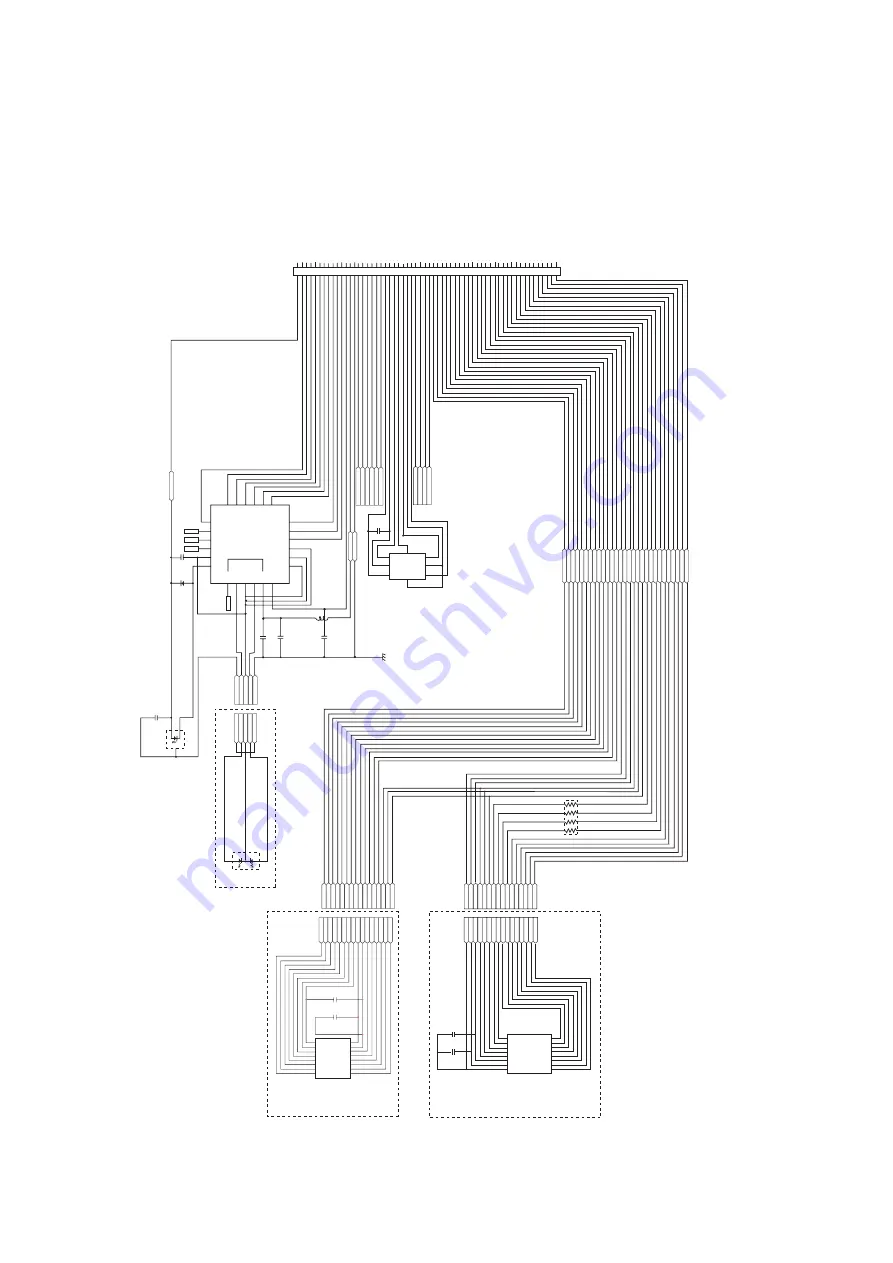
INTERNAL STRUCTURE OF THE PICK-UP
1. Block Diagram of the PICK-UP(JPA27Z)
22
SW2
Vtc
Vref
GND
B4C4
B2C2
SL
SW1
B1C1
B3C3
A1
A3
RFP
RFN
A4
A2
A2
A4
RFP
RFN
A1
A3
SW2
Vcc
V
ref
GND
B4C4
B2C2
SL
SW1
B1C1
B3C3
V
ref
GND
Vcc
GS1
B1
B6
A3
A4
A2
A1
GS2
RFN
RFP
SLEEP
B3
B5
C3
0.1u
C4
0.1u
2W_OEIC
A3
A4
A2
A1
GS2
RFN
RFP
SLEEP
B3
B5
B1
B6
Vtc
GS1
GND
Vref
BD_OEIC
C1
0.1u
BR1
22
C2
0.1u
IC3
L
V0318XA
IC4
PNA4T19F01
A2
A4
RFP
RFN
A1
A3
SW2
Vcc
V
ref
GND
B4C4
B2C2
SL
SW1
B1C1
B3C3
F01-(ACT)
F01+(ACT)
T
r+(ACT)
T
r-(ACT)
SA-(STPM)
SB+(STPM)
SB-(STPM)
SA+(STPM)
IOUT2
GND
GND
IOUT1
GND
F02+(ACT)
F02-(ACT)
V
ref
GND
Vcc
GS1
B1
B6
A3
A4
A2
A1
GS2
RFN
RFP
SLEEP
B3
B5
A2
A4
GND
LD+
Vcc
IC2
CPF274ALK
ISL58797
IC1
C6
0.1u
C7
2.2u
BD_LD
CD_LD
GND
DVD_LD
C1
1
68000p(10V)
L1
C9
FG
2200p
80Ω@100MHz
1u(10V)
C10
CN60P
LD+
BSEL(LDD)
ENA(LDD)
SEN(LDD)
SDIOO(LDD)
SCLK(LDD)
WEB(LDD)
WEN(LDD)LDD)
WEN0B(LDD)
WEN1(LDD)
WEN1B(LDD)
IAPC(LDD)
GND(LDD)
Vcc(LDD)
F02+(ACT)
F02-(ACT)
T
r+(ACT)
T
r-(ACT)
F01-(ACT)
F01+(ACT)
Vcc(FSPD)
GND(FSPD)
ENB(FSPD)
DA
T
A(AFSPD)
CLK(FSPD)
OUTP(FSPD)
OUTN(FSPD)
SB+(STPM)
SA+(STPM)
SA-(STPM)
SB-(STPM)
A4(2W)
A2(2W)
RFP(2W)
RFN(2W)
A1(2W)
A3(2W)
SW2(2W)
Vcc(2W)
V
ref(2W)
GND(2W)
B4C4(2W)
B2C2(2W)
SL(2W)
GND(BD)
V
ref(BD)
Vcc(BD)
GS1(BD)/SW1(2W))
B1(BD)/B1C1(2W)
B6(BD)/B3C3(2W)
A3(BD)
A4(BD)
A2(BD)
A1(BD)
GS2(BD)
RFN(BD)
RFP(BD)
SLEEP(BD)
B3(BD)
B5(BD)
60
59
58
57
56
55
54
53
52
51
50
49
48
47
46
45
44
43
42
41
40
39
38
37
36
35
34
33
32
31
30
29
28
27
26
25
24
23
22
21
20
19
18
17
16
15
14
13
12
11
10
9
8
7
6
5
4
3
2
1
D1
8
13
14
15
16
17
18
6
5
4
2
3
1
4
5
6
3
7
8
9
10
11
12
ENB
BSEL
GC1
GC2
MC
GND
IBLUE
connected on die
CLK
WEN0B
WEN1
WEN1B
WEN2
WEN2B
ISLCPE
NC
CUTN
GND
Vtc
2
21
20
19
22
23
24
1
7
C5
DA
T
AOUTP
WEN0
WEB
IAPC
VSO
VSO
IOUT2
IOUT1
GND
SCLK
SDIO
SEB
ENA
0.1u
RFP
RFN
A1
A3
SW2
Vcc
V
ref
GND
B4C4
B2C2
SL
V
ref
GND
Vcc
A3
A4
A2
A1
GS2
RFN
RFP
SLEEP
B3
B5
GS1/SW1
B1/B1C1
B6/B3C3
NC
NC
NC
NC
DVD LD
GND
GND
CD LD
GND
Summary of Contents for BP50NB40
Page 17: ...17 A B C 1 2 3 4 5 A00 A01 002 003 461 005 001 463 006 462 004 PBM01 B B EXPLODED VIEW ...
Page 23: ...23 2 CONNECTOR 66 PIN ASSIGNMENT ...
Page 24: ...24 ...
Page 29: ...29 3 1 2 Block Diagram Seek IC101 MT1959H ...
Page 34: ...1 2 Pin Layout RF Part 34 ...
Page 35: ...35 ...
Page 36: ...36 ...
Page 37: ...37 ENDEC Part ...
Page 38: ...38 ...
Page 39: ...39 ...
Page 40: ...40 ...
Page 41: ...41 ...
Page 42: ...42 ...
Page 43: ...43 ...
Page 44: ...44 ...
Page 45: ...45 IC601 TPIC2016G SPINDLE MOTOR AND 10CH ACTUATOR DRIVER Terminal Assignments ...