LGE Internal Use Only
Copyright © 2007 LG Electronics. Inc. All right reserved.
Only for training and service purposes
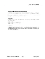
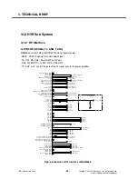
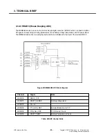
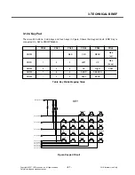
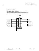
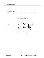
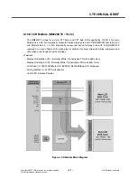
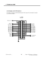
3.12 H/W Sub System
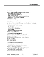
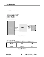
3.12.1 RF Interface
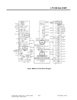
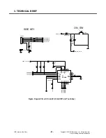
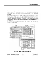
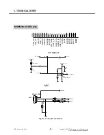
A. RTR6275(WCDMA_Tx, GSM_Tx/Rx)
MSM6260 controls RF part(RTR6275) using these signals.
• SBST : SSBI I/F signals for control Sub-chipset
• PA_ON1, PA_ON2 : Power AMP on RF part
• RX0_I/Q_M/P,TX_I/Q_M/P: I/Q for T/Rx of RF
• TX_AGC_ADJ : control the gain of the Tx signal prior to the power amplifier
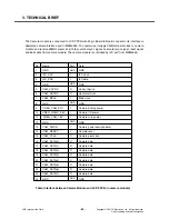
3. TECHNICAL BRIEF
- 36 -
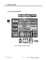
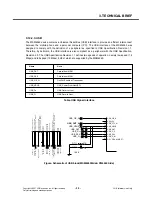
Figure. Schematic of RF Interface of MSM6260
W1900 PAM
W850 PAM
Close to MSM
2K
R211
33nF
C240
TP202
XMEM1_CS_N1_GPIO76
XMEM1_CS_N3_SDRAM1_CS_N1_GPIO77
Y6
W15
XMEM2_CS_N2_GPIO35
AA15
XMEM2_CS_N3_GPIO36
L25
UART3_RFR_N_GPIO87
USB_RX_DATA_GPIO29
N19
WDOG_STB_SBCK1_GPIO0
H25
AA1
A17
TMS
F15
TRK_LO_ADJ
L13
H15
TRST_N
H13
TX_AGC_ADJ
TX_ON_GRFC10
H12
H6
UART2_DP_RX_DATA_GPIO89
F18
SYNTH0_GP_PDM0_GPIO92
B6
SYNTH2_GPIO65
TCK
D16
TCXO_EN_GPIO94
F19
D15
TDI
TDO
SBDT1_GPIO1
SBST1_GPIO93
H18
AA25
Q_IM_CH0
Q_IM_CH1
W23
Y25
Q_IP_CH0
Q_IP_CH1
V23
B12
Q_OUT
A12
Q_OUT_N
RTCK
H16
F26
PA_ON0
F17
H11
PA_ON1_GPIO2
AB25
I_IM_CH0
V25
I_IM_CH1
AC25
I_IP_CH0
W25
I_IP_CH1
I_OUT
B13
I_OUT_N
A13
AE13
LCD_EN_GPIO37
GRFC5_AUX_SBST_GPIO8
GRFC7_GPIO10
T23
B4
GRFC8_GPIO11
D5
GRFC9_GPIO12
GRFX6_GPIO9
T19
GPIO66
H17
GP_PDM1_PA_RANGE0
D17
GP_PDM2_PA_RANGE1
B8
GRFC0_GPIO3
A8
GRFC1_AUX_SBDT_GPIO4
D9
GRFC2_GPIO5
F10
GRFC3_GPIO6
GRFC4_AUX_SBCK_GPIO7
H10
D11
A6
GPIO28
H9
GPIO43
F8
F12
DAC_REF
AUX_PCM_CLK_GRFC14_GPIO80
K19
N21
AUX_PCM_DIN_GRFC13_GPIO14
AUX_PCM_DOUT_GRFC12_GPIO103
G4
AUX_PCM_SYNC_GRFC11_GPIO102
J8
CAMCLK_PO_GP_MN_GPIO13
J21
CAM_LDO_EN
JTAG_TCK
VGA_CAM_RESET
TFLASH_DET_N
PA_ON2
PA_ON1
SPK_SW_ON
SPK_AMP_EN
ANT_SEL3
CAM_MCLK
GSM_SAW_SW_MODE
GSM_PA_BAND
GSM_PA_EN
PA_R0
LCD_RESET_N
LCD_IF_MODE
DAC_REF
TX_IM
TX_IP
RX_IP
RX_IM
ANT_SEL0
ANT_SEL2
ANT_SEL1
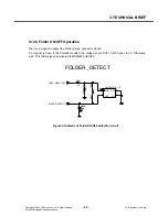
FOLDER_DETECT
HOOK_SENSE_N
TCXO_EN
JTAG_TDI
JTAG_TDO
JTAG_TMS
JTAG_TRST_N
TX_AGC_ADJ
TX_ON
CAM_PWDN
TRK_LO_ADJ
RX_QM
RX_QP
TX_QP
TX_QM
JTAG_RTCK


