background image

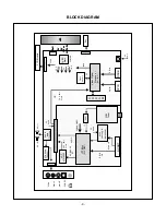
DESCRIPTION OF BLOCK DIAGRAM

- 10 -

1. Format Converter (MST9883C)(U702)

This IC contain A/D converter, Pre-amp and PLL circuit that converting.
Analog video signal(0.7p-p RGB) to digital signal.(656 Format)

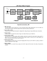
2. Power Supply Block (LIPS)

This Block Generates DC Voltage (5V,15V) to Main Control system from AC Power (100-240V, 50/60Hz, 1.0A)
The Minimum of Power efficiency is about 80%.

3. DC/DC Converter block

DC/DC Converter convert the input 5V,15V to proper  3.3V,5V,12V for Main control system.
For shooting heat trouble, we use the DC/DC converting IC

4. Audio Amplifier (TPA3004D2)(U201)

This block is composed of TPA3004D2 and peripheral device
The function of the audio amplifier is that to amplify audio L / R signal transmitted from audio decoder.
The audio signal is amplified according to pre-defined DC volume control curve. Also, headphone amplifier (TPA6110) is
controlled through line-out.

5. Audio / Video / IF Decoder(U601)

This block is composed of VCT49xy and peripheral devices.
Micom controls this IC through IIC Line.

1) Video Decoder

This Block Selects input Video signals (like CVBS, Y/C, SCART RGB) and output RGB signal.
On decoding, We can control signal like Contrast, Brightness, Sharpness, Color, tint signals including Adaptive Comb
Filter.

2) Audio Decoder

This block analyzes audio input signal through A/V Jack and PC audio and Tuner IF.
The analyzed signals transmitted to audio amplifier (TPA3004D2)
On decoding, We can control signal like Bass, treble.

3) IF Decoder

This block can change IF signal to audio and video signal that transmitted to Video/audio decoder.

6.Video signal processor (Scaler IC) (U401)

It is composed of GM1501
Micom control this IC through IIC Line.
This IC include A/D converter for PC input and LVDS Transmitter.
This IC is directly inputted Analog and Digital Signal and transmits to LCD Module.

7. Micom (4M Flash Memory) (U403)

It is composed of AT49BV040A.
This IC controls peripheral devices through IIC line.

8. TUNER(TU802)

Micom controls this IC through IIC Line.
TUNER makes IF and transmits IF signal to VCT49xy.

Summary of Contents for flatron M1740A

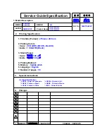
Page 1: ...36 Part No 1 2 Service Guide Specification Service Guide Specification Changes 4 REV NO MM DD YY SIGNATURE CHANGE NO CHANGE CONTENTS 1 2 3 4 5 7 6 SUFFIX LEE H J 05 12 30 M1740A RZB M1940A RZB M2040A RZB LG 3828TSL094P KIM J O 05 12 30 1 Origin Notification LGEDI Printed in Indonesia LGEWA Printed in U K LGESP Printed in Brazil LGEMX Printed in Mexico LGENT Printed in China LGEIL Printed in India ...

Page 2: ...eet Pagination sheet P NO 3828TSL094P Total pages 36pages Cover English 3 English 4 English 5 English English Rear Cover Front cover Inside 2 English English 31 English 32 English 33 English 34 Rear cover Inside 35 ...

Page 3: ...ite http biz LGservice com E mail http www LGEservice com techsup html CAUTION BEFORE SERVICING THE UNIT READ THE SAFETY PRECAUTIONS IN THIS MANUAL CHASSIS NO CL 75 MODEL M1740A M1740A RZB AN LF M1940A M1940A RZB AN LF M2040A M2040A RZB AL LF Same model for Service ...

Page 4: ...r IF PIF 38 9MHz SIF 33 4MHz CIF 34 47MHz 3 Receiving Channel VHF Low 45 25 140 25MHz HIGH 147 25 423 25MHz UHF 431 25 855 25MHz 4 4 AV 1 Video Level Input 0 7 0 15Vp p 2 Sync Level Input 0 286 0 075Vp p 3 Color Burst Input 0 214 0 072Vp p 4 Audio Level AV Input 0 5 0 1Vrms PC Input 0 7 0 1Vrms 5 Video Cross Talk 43dB 5 Max Resolution SXGA 1280 x 1024 75Hz M1740A M1940A VXGA 1600 x 1200 60Hz M2040...

Page 5: ...e module from the ESD as it may damage the electronic circuit C MOS Make certain that treatment person s body are grounded through wrist band Do not leave the module in high temperature and in areas of high humidity for a long time The module not be exposed to the direct sunlight Avoid contact with water as it may a short circuit within the module If the surface of panel become dirty please wipe i...

Page 6: ...t receiver ground lead to the receiver chassis ground before connecting the test receiver positive lead Always remove the test receiver ground lead last 9 Use with this receiver only the test fixtures specified in this service manual CAUTION Do not connect the test fixture ground strap to any heat sink in this receiver Electrostatically Sensitive ES Devices Some semiconductor solid state devices c...

Page 7: ...tip as the solder melts 2 Draw away the melted solder with an anti static suction type solder removal device or with solder braid before removing the IC Replacement 1 Carefully insert the replacement IC in the circuit board 2 Carefully bend each IC lead against the circuit foil pad and solder it 3 Clean the soldered areas with a small wire bristle brush It is not necessary to reapply acrylic coati...

Page 8: ...onnection 4 Route the jumper wire along the path of the out away copper pattern and let it overlap the previously scraped end of the good copper pattern Solder the overlapped area and clip off any excess jumper wire At Other Connections Use the following technique to repair the defective copper pattern at connections other than IC Pins This technique involves the installation of a jumper wire on t...

Page 9: ...152 832 32 64 224 832 x 624 V Lines 74 55 667 624 1 3 39 8 H Pixels 65 0 48 363 1344 1024 24 136 160 1024 x 768 V Lines 60 0 806 768 3 6 29 9 H Pixels 78 75 60 123 1312 1024 16 96 176 1024 x 768 V Lines 75 029 800 768 1 3 28 10 H Pixels 100 0 68 681 1456 1152 32 128 144 1152 x 870 V Lines 75 062 915 870 3 3 39 11 H Pixels 92 978 61 805 1504 1152 18 134 200 1152 x 900 V Lines 65 96 937 900 2 4 31 1...

Page 10: ... 8 DISASSEMBLY Disassembly Hinge Cover Open the Backcover s latch with Jig Disassemble back cover Remove the 4 screws of metal frame Remove the screws Remove the screws 1 4 2 5 3 6 ...

Page 11: ...5 5 5 V V V V 5 5 5 5 V V V V I I I I N N N N V V V V o o o o n n n n B B B B R R R R T T T T A A A A D D D D J J J J 33 V 15 V 5 V 3 3 V 1 8 V Video Signal Process or Gm1501CF DVI D DSUB Digital PC Audio Flash memory R G B IIC S D R A M IIC POWER IF CVBS S VIDEO VCTi49xy A V DEC SCART SAW Audio L R W W Tuner IIC RGB HS VS LVDS YUV 8bit Clock R G B FB Audio switc hing IC MC140 66B PC Audio PC Audi...

Page 12: ...is block is composed of VCT49xy and peripheral devices Micom controls this IC through IIC Line 1 Video Decoder This Block Selects input Video signals like CVBS Y C SCART RGB and output RGB signal On decoding We can control signal like Contrast Brightness Sharpness Color tint signals including Adaptive Comb Filter 2 Audio Decoder This block analyzes audio input signal through A V Jack and PC audio ...

Page 13: ... bridge rectifier and a bulk capacitor 3 Energy Transfer This part function is for transfer the primary energy to secondary through a power transformer 4 Output rectifier and filter This part function is to make a pulse width modulation control and to provide the driver signal to power switch to adjust the duty cycle during different AC input and output loading condition to achieve the dc output s...

Page 14: ...anufacture Serial Number a Input User Info Data b Click Update button c Click Write button EEPROM initialize COMMAND 0xE4 0x00 0x00 ADC adjustment Black COMMAND 0xF1 0x00 0x00 ADC adjustment white COMMAND 0xF1 0x00 0x01 AV Mode ADC adjustment Red COMMAND 0x16 0x00 0x00 0x00 FF ADC adjustment Green COMMAND 0x18 0x00 0x00 0x00 FF ADC adjustment Blue COMMAND 0x1A 0x00 0x00 0x00 FF Factory shipping co...

Page 15: ...pe Polish France Scandinavian Czech Slovak German Slovenian Croatian Italian Rumanian Recommended data TURKEY W EU Recommended data English France Scandinavian Turkish German Spain Portuguese Italian Greek English Czech Hungary German Polish Serbia Turkish Rumanian CYRILLIC 1 Polish Russian Estonian Lettish Estonian CYRILLIC 2 Polish Russian Scandinavian Czech Estonian Lettish CYRILLIC 3 Recommend...

Page 16: ...t Switch 110V 220V Control Line N o t u s e d R S 2 3 2 C P A R A L L E L V S Y N C P O W E R S T VGS MONITOR E E V Sync On Off Switch Switch must be ON F F A A B B C C 15 10 5 5 6 9 1 1 1 14 13 25 6 5V 5V 5V 4 7K 4 7K 4 7K 74LS06 74LS06 OFF ON OFF ON 11 ANT IN PC Audio D Audio R Audio L S Video Video Signal Generator ...

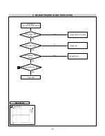
Page 17: ...em Around U903 U906 NO Check U402 YES YES CHECK J901 Voltage Pin 1 2 15V Pin 5 6 5V Check U903 Pin 3 3 3V Check U906 Pin 3 1 8V Check X401 14 318Mhz 1 2 3 4 5 1 2 Waveforms J901 1 2 15V J901 5 6 5V 4 5 U906 3 1 8V X401 14 318Mhz 3 U903 3 3 3V TROUBLESHOOTING GUIDE 1 NO POWER NO POWER POWER INDICATOR OFF YES YES ...

Page 18: ...AYED NO RASTER OSD IS NOT DISPLAYED NO NO Change J401 NO Change Pannel Link Cable Change Micom YES YES YES YES Check Pannel Link Cable Check J401 Crack Check Micom ID Version Check U918 Pin 2 2 5V Check U402 6 Waveforms U918 2 2 5V 6 ...

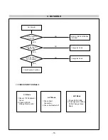
Page 19: ... Board Ass y YES Check Cable of J106 Check Video Board Check U908 Pin 1 3 5V 3 3V Check U909 Pin 3 1 8V In Case of AV1 Scart In Case of TV NO Change Video Board Ass y NO YES Check Peripheral Circuit YES YES Check Tuner TU802 Check Connection of EXT YES 7 8 9 Waveforms 7 8 9 U908 1 5V U908 3 3 3V U909 3 1 8V YES ...

Page 20: ... 8V AV1 Mode 1 Check Scart Connection 2 Check No Raster AV1 AV2 Mode 1 Check C605 C606 2 If No Signal on C605 or C606 Change Video Board YES Check a Signal of C153 156 Check the Cable of Main to Key NO Check the Cable of Key to Speaker CHECK INPUT SIGNAL CHECK THE PERIPHERAL ICOf U201 Change the Cable Change the Cable YES YES ...

Page 21: ... 19 L R 11P 12P 8P 12P 30P 6631T20023J 6631T11012W M1740A M1940A 6631T11020N M2040A 6400ZTTE01A M1740A M1940A 6400ZTTS01A M2040A 6631T20028U 6631T12006T 6631T12006U WIRING DIAGRAM ...

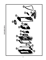
Page 22: ... 20 EXPLODED VIEW 010 050 060 070 020 080 090 100 110 120 030 150 130 140 040 ...

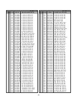
Page 23: ...3TKK230F TILT SWIVEL ASSEMBLY M1940A SILVER E CKD M2040A 6400ZTTE01A SPEAKER FULLRANGE KTA N1040 1 TOPTONE OTHERS 16OHM 3 5W DB 100 TW WF M1740A M1940A 6400ZTTS01A SPEAKER FULLRANGE KTA N1527 1 TOPTONE OTHERS 16OHM 5 7W DB 70 TW WF M2040A 6871TST914A PWB PCB ASSEMBLY SUB M1740A M1940A M2040A CONTROL TOTAL BRAND KEY 6871TSP685B PWB PCB ASSEMBLY SUB M1740A M1940A M2040A LED P SW SMD TOP BRAND TOUCH ...

Page 24: ... DESCRIPTION SPECIFICATION C220 0CK105CF94A 1UF 1608 16V 80 20 R TP F C221 0CH3105H946 1UF 2012 25V 80 20 F Y5V C222 0CK105CF94A 1UF 1608 16V 80 20 R TP F C223 0CK105CF94A 1UF 1608 16V 80 20 R TP F C224 0CK105CF94A 1UF 1608 16V 80 20 R TP F C225 0CH3105H946 1UF 2012 25V 80 20 F Y5V C226 0CH8476H691 47UF 25V 20 105STD CYL R C227 0CH8476H691 47UF 25V 20 105STD CYL R C228 0CH3474H946 0 47UF 25V 80 20...

Page 25: ...F610 100UF KMG RD 16V 20 FL BULK C654 0CH3104K566 0 1UF 50V 10 X7R 2012 R TP C655 0CH3104K566 0 1UF 50V 10 X7R 2012 R TP DATE 2005 11 30 S AL LOC NO PART NO DESCRIPTION SPECIFICATION C656 0CH3104K566 0 1UF 50V 10 X7R 2012 R TP C657 0CH3104K566 0 1UF 50V 10 X7R 2012 R TP C658 0CH3104K566 0 1UF 50V 10 X7R 2012 R TP C659 0CH3104K566 0 1UF 50V 10 X7R 2012 R TP C660 0CH6220K416 22PF 2012 50V 5 NP0 C661...

Page 26: ...0 1 R TP X7R DATE 2005 11 30 S AL LOC NO PART NO DESCRIPTION SPECIFICATION C973 0CK103CK51A 0 01UF 1608 50V 10 R TP B Y C974 0CE107EF610 100UF KMG RD 16V 20 FL BULK C975 0CK104CK56A 0 1UF 1608 50V 10 R TP X7R C976 0CK225DH94A 2 2UF 2012 25V 80 20 F Y5 M2040A C978 0CK475FH67A 4 7UF 3225 25V 20 X5R R TP M2040A D101 0DSIH00018A ENKMC2837 T112 LF ISAHAYA R X7R M1710A M1910A D101 0DS226009AA KDS226 TP ...

Page 27: ...012 301JT CERATEC 2012 L813 6210TCE001H HB 1T2012 301JT CERATEC 2012 DATE 2005 11 30 S AL LOC NO PART NO DESCRIPTION SPECIFICATION L814 6210TCE001H HB 1T2012 301JT CERATEC 2012 L815 6210TCE001H HB 1T2012 301JT CERATEC 2012 L816 6210TCE001H HB 1T2012 301JT CERATEC 2012 L101 6210TCE001Y HB 1H2012 320JT CERATEC 2012 L102 6210TCE001Y HB 1H2012 320JT CERATEC 2012 L103 6210TCE001G HH 1M3216 501 CERATEC ...

Page 28: ... R TP M2040A R220 0RJ2002D677 20000 OHM 1 10 W 5 1608 R T X7R M1710A M1910A R220 0RJ1002D677 10K OHM 1 10 W 5 1608 R TP M2040A DATE 2005 11 30 S AL LOC NO PART NO DESCRIPTION SPECIFICATION R221 0RH0000D622 0 OHM 1 10 W 2012 5 00 D R222 0RH0000D622 0 OHM 1 10 W 2012 5 00 D R223 0RH1001D622 1K OHM 1 10 W 2012 5 00 D R224 0RH1001D622 1K OHM 1 10 W 2012 5 00 D R225 0RH1002D622 10K OHM 1 10 W 2012 5 00...

Page 29: ... 5 1608 R TP R620 0RJ0000D677 0 OHM 1 10 W 5 1608 R TP R621 0RH2700D622 270 OHM 1 10 W 2012 5 00 DATE 2005 11 30 S AL LOC NO PART NO DESCRIPTION SPECIFICATION R622 0RH2700D622 270 OHM 1 10 W 2012 5 00 R623 0RH2700D622 270 OHM 1 10 W 2012 5 00 R624 0RH0000D622 0 OHM 1 10 W 2012 5 00 D R625 0RH1001D622 1K OHM 1 10 W 2012 5 00 D R627 0RH1000D622 100 OHM 1 10 W 2012 5 00 R630 0RH1000D622 100 OHM 1 10 ...

Page 30: ... R922 0RJ1001D677 1K OHM 1 10 W 5 1608 R TP R923 0RJ1002D677 10K OHM 1 10 W 5 1608 R TP R924 0RJ1001D677 1K OHM 1 10 W 5 1608 R TP DATE 2005 11 30 S AL LOC NO PART NO DESCRIPTION SPECIFICATION R925 0RB0470K607 0 47 OHM 2 W 5 TA62 R926 0RB0470K607 0 47 OHM 2 W 5 TA62 R927 0RJ0000D677 0 OHM 1 10 W 5 1608 R TP X7R M1710A M1910A R928 0RJ2202D677 22K OHM 1 10 W 5 1608 R TP X7R M1710A M1910A R929 0RJ560...

Page 31: ...CK41A 470PF 1608 50V 5 R TP NP0 C703 0CC471CK41A 470PF 1608 50V 5 R TP NP0 C704 0CC331CK41A 330PF 1608 50V 5 R TP NP0 C706 0CK104CK56A 0 1UF 1608 50V 10 R TP X7R C707 0CK104CK56A 0 1UF 1608 50V 10 R TP X7R L701 6210TCE001H HB 1T2012 301JT CERATEC 2012 L702 6210TCE001H HB 1T2012 301JT CERATEC 2012 L703 6210TCE001H HB 1T2012 301JT CERATEC 2012 L704 6210TCE001H HB 1T2012 301JT CERATEC 2012 L705 6210T...

Page 32: ...SCHEMATIC DIAGRAM 30 1 CONNECTOR JACK ...

Page 33: ... 31 2 MEMORY AUDIO AMP ...

Page 34: ... 32 3 SCALER GM1601 5 X401 14 318Mhz 5 Waveforms ...

Page 35: ... 33 4 VUDEO DEC VCT49XYI ...

Page 36: ... 34 5 MST9883C TUNER SCARTJACK ...

Page 37: ... 35 6 POWER 6 1 4 3 U903 3 3 3V 3 7 9 8 4 U906 3 1 8V 6 U918 2 2 5V 7 U908 1 5V Waveforms 1 J901 1 2 15V 2 J901 5 6 5V 8 9 U908 3 3 3V U909 3 1 8V 2 ...

Page 38: ...Nov 2005 P NO 3828TSL094P Printed in Korea ...

Reviews: