38
The integrated power management also provides the control state machine for system start up,
including start up with discharged batteries, pre-charging and system reset control.
After system start up several methods are implemented for active and idle power saving.
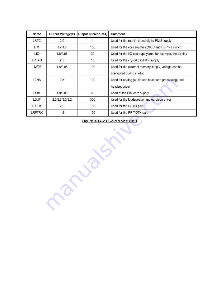
LDO output voltage selection
• LD1, LIO, LSIM, LBUF output voltage programmable by software.
• LMEM output voltage is selectable by pin configuration upon startup.
Active and idle power saving options:
• The flexible clock switching options allow minimizing the power consumption during the
operation phases of the E-GOLDvoice.
• Current consumption during the standby mode is minimized by reducing the clock to 32 kHz and
switching it off for most of the device. In addition, the power supply for the TEAKLite ROM is
switched off and the controller RAM is switched to a power saving mode.
Start-up and Reset Control State Machine Features
• Power up upon battery insertion, push button, alarm, charger connection.
• Detection of battery exchange or re-insertion.
• Complete start-up sequence management.
• System turn-on, system turn-off operation management including emergency (under-voltage)
and programmed shutdown functions.
• Internal reset of the baseband.
• Tristate function of the baseband module.
• Standby mode controlled by VCXO_EN provided by SCCU module.
Summary of Contents for GB108
Page 1: ...1 GB108 Service Manual LG Electronics ...
Page 11: ...11 3 TECHNICAL BRIEF Digital Main Processor Figure 3 1 PMB7880 FUNCTIONAL BLOCK DIAGRAM ...
Page 12: ...12 ...
Page 22: ...22 RTC 32 768KHz Crystal Figure 3 4 E GoldVoice RTC Interface ...
Page 24: ...24 ...
Page 25: ...25 3 6 SIM Card Interface Figure 3 6 SIM CARD Interface ...
Page 26: ...26 3 7 KEYPAD Interface Figure 3 7 KEY MAXTRIX Interface ...
Page 27: ...27 3 8 Battery Charging Block Interface Figure 3 8 Charging IC Interface ...
Page 28: ...28 3 9 RF Interface Figure 3 9 RF Module SAW Filter Interface ...
Page 29: ...29 ...
Page 30: ...30 3 10 Audio Interface Figure 3 10 1 Audio Interface ...
Page 31: ...31 ...
Page 32: ...32 Figure 3 10 2 Main Speaker Receiver Interface ...
Page 33: ...33 Figure 3 10 3 Main Microphone Interface Figure 3 10 4 Headset Interface ...
Page 36: ...36 3 13 Memory Interface Figure 3 13 Memory Interface ...
Page 39: ...39 3 15 FM Radio Interface GB105a b GB106 GB107a b GB108 only Figure 3 15 FM Radio Interface ...
Page 41: ...41 ...
Page 42: ...42 PAM Matching component Mobile SW Antenna Matching component Antenna connect point ...
Page 43: ...43 ...
Page 44: ...44 ...
Page 45: ...45 ...
Page 46: ...46 ...
Page 47: ...47 ...
Page 48: ...48 TP2 TP1 TP3 ...
Page 49: ...49 TP2 TP1 TP3 ...
Page 50: ...50 ...
Page 52: ...52 Circuit Diagram TP5 TP6 TP1 TP3 TP4 TP2 ...
Page 54: ...54 4 4 SIM Card Trouble Test Point Circuit Diagram ...
Page 56: ...56 4 5 Vibrator Trouble Test Point Circuit Diagram ...
Page 58: ...58 4 6 Keypad Trouble Test Point Circuit Diagram ...
Page 59: ...59 Checking Flow Change Metal Dome Check Metal Dome Start Change PCB NG OK ...
Page 60: ...60 4 7 RTC Trouble Test Point Circuit Diagram ...
Page 62: ...62 4 8 Key Backlight Trouble Test Point ...
Page 63: ...63 Circuit Diagram ...
Page 65: ...65 4 9 LCM Backlight Trouble Test Point Circuit Diagram ...
Page 67: ...67 4 10 LCM Trouble Test Point Circuit Diagram ...
Page 69: ...69 4 11 Microphone Trouble Test Point Circuit Diagram ...
Page 71: ...71 4 12 Receiver Trouble Test Point Circuit Diagram ...
Page 73: ...73 4 13 Speaker Trouble Test Point Circuit Diagram TP6 TP5 TP2 TP3 TP4 TP1 ...
Page 75: ...75 4 14 Headphone Trouble Test Point ...
Page 76: ...76 Circuit Diagram TP1 TP2 ...
Page 79: ...79 4 15 Charging Trouble Test Point Circuit Diagram ...
Page 81: ...81 4 16 FM Radio Trouble GB105a b GB106 GB107a b only Test Point ...
Page 82: ...82 Circuit Diagram ...
Page 86: ...86 5 DOWNLOAD 5 1 Download Setup ...
Page 91: ...91 6 BLOCK DIAGRAM ...
Page 92: ...92 ...
Page 93: ...93 ...
Page 94: ...94 ...
Page 95: ...95 ...
Page 96: ...96 ...
Page 97: ...97 ...
Page 99: ...99 BGA PIN Check of Memory Top View Use U201 Memory S71GL032N40BFW0P Not Use EUSY0328002 ...
Page 100: ...100 9 PCB LAYOUT ...
Page 105: ...105 11 Calibration 11 1 Test equipment setup 11 2 Calibration Steps Execute HK_36 exe ...
Page 107: ...107 Select MODEL Click START for RF calibration RF Calibration finish ...
Page 113: ...113 13 EXPLODED VIEW REPLACEMENT PART LIST 13 1 Exploded View GB108 ...
Page 114: ...114 ...


