15
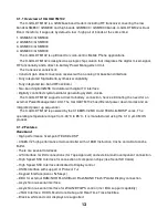
3.1.3 System Platform Application
X-GOLDTM102 was developed for very low cost Dual Band GSM/GPRS system solutions.
Here are some potential System Platform configurations that can be built with X-GOLDTM102
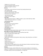
Solution:
3.1.4 GSM System Description
The X-GOLDTM102 is suited for mobile stations operating in the GSM850/900/1800/1900 bands.
In the receiver path the antenna input signal is converted to the baseband, filtered, and then
amplified to target level by the RF transceiver chip set. Two A-to-D converters generate two 6.5
Mbit/s data streams. The decimation and narrowband channel filtering is done by a digital
baseband filter in each path. The DSP performs:
1. The GMSK equalization of the received baseband signal (SAIC support available)
2. Viterbi channel decoding supported by an hardware accelerator.
The recovered digital speech data is fed into the speech decoder. The X-GOLDTM102 supports
fullrate, halfrate, enhanced fullrate and adaptive multirate speech CODEC algorithms.
The generated voice signal passes through a digital voiceband filter. The resulting 4 Mbit/s data
stream is D-to-A converted by a multi-bit-oversampling converter, postfiltered, and then amplified
by a programmable gain stage.
The output buffer can drive a handset ear-piece or an external audio amplifier, an additional output
driver for external loud speaker is implemented.
In the transmit direction the differential microphone signal is fed into a programmable gain amplifier.
The prefiltered and A-to-D converted voice signal forms a 2 Mbit/s data stream. The oversampled
voice signal passes a digital decimation filter.
The X-GOLDTM102 performs speech and channel encoding (including voice activity detection
(VAD) and discontinuous transmission (DTX)) and digital GMSK modulation.
In the RF transceiver part, the baseband signal modulates the RF carrier at the desired frequency
in the 850 MHz, 900 MHz, 1.8 GHz, and 1.9 GHz bands using an I/Q modulator. The
X-GOLDTM102 supports dual band applications.
Finally, an RF power module amplifies the RF transmit signal at the required power level. Using
software, the X-GOLDTM102 controls the gain of the power amplifier by predefined ramping curves
(16 words, 11 bits).
Summary of Contents for GB130kf750
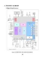
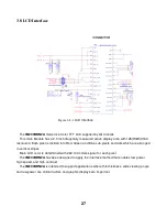
Page 12: ...12 3 TECHNICAL BRIEF 3 1Digital Main Processor Figure 3 1 PMB7890 FUNCTIONAL BLOCK DIAGRAM ...
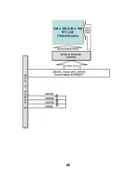
Page 28: ...28 ...
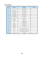
Page 29: ...29 Pin Description ...
Page 35: ...35 Circuit Diagram TP1 TP6 TP2 TP4 TP 3 TP5 ...
Page 36: ...36 Checking Flow ...
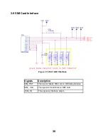
Page 37: ...37 4 2 SIM Card Trouble Test Point Circuit Diagram ...
Page 38: ...38 Checking Flow ...
Page 39: ...39 4 3 Vibrator Trouble Test Point Circuit Diagram ...
Page 40: ...40 Checking Flow NG ...
Page 41: ...41 4 4 Keypad Trouble Test Point ...
Page 42: ...42 Circuit Diagram ...
Page 43: ...43 ...
Page 44: ...44 Checking Flow ...
Page 45: ...45 4 5 RTC Trouble Test Point Circuit Diagram ...
Page 46: ...46 Checking Flow ...
Page 47: ...47 4 6 Key Backlight Trouble 4 6 1 Main Key Board LED ...
Page 48: ...48 Circuit Diagram Checking Flow ...
Page 49: ...49 4 6 2 Upper Key Board LED Circuit Diagram TP1 ...
Page 50: ...50 Checking Flow ...
Page 51: ...51 4 7 LCM Backlight Trouble Test Point Circuit Diagram ...
Page 52: ...52 Checking Flow ...
Page 53: ...53 4 8 LCM Trouble Test Point Circuit Diagram ...
Page 54: ...54 Checking Flow ...
Page 55: ...55 4 9 Microphone Trouble Test Point Circuit Diagram TP1 ...
Page 56: ...56 Checking Flow ...
Page 57: ...57 4 10 Receiver Trouble Test Point ...
Page 58: ...58 Circuit Diagram ...
Page 59: ...59 Checking Flow ...
Page 60: ...60 4 11Speaker Trouble Test Point ...
Page 61: ...61 Circuit Diagram ...
Page 62: ...62 Checking Flow ...
Page 63: ...63 4 12 Headphone Trouble Test Point Circuit Diagram ...
Page 64: ...64 ...
Page 65: ...65 Checking Flow ...
Page 66: ...66 ...
Page 67: ...67 4 13 Charging Trouble Test Point Circuit Diagram TP1 TP4 TP3 TP5 TP2 ...
Page 68: ...68 Checking Flow ...
Page 69: ...69 4 14 FM Radio Trouble Test Point ...
Page 70: ...70 Circuit Diagram ...
Page 71: ...71 Checking Flow ...
Page 72: ...72 ...
Page 74: ...74 RF Trouble TEST POINT ...
Page 76: ...76 ...
Page 77: ...77 RX Trouble TEST POINT ...
Page 78: ...78 CIRCUIT TP5 TP6 TP3 TP4 TP1 TP2 ...
Page 79: ...79 CHECKING FLOW ...
Page 80: ...80 TEST POINT CIRCUIT TP1 TP2 TP5 TP6 TP3 TP4 TP2 TP1 ...
Page 81: ...81 WAVE FORM CHECKING FLOW Replace X301 ...
Page 82: ...82 TX Trouble TEST POINT ...
Page 83: ...83 CIRCUIT WAVE FORM TP5 TP6 TP3 TP4 TP2 TP1 ...
Page 84: ...84 TEST POINT ...
Page 85: ...85 CHECKING FLOW ...
Page 86: ...86 Signal configuration CHECKING FLOW ...
Page 87: ...87 TROUBLE SHOOTING TEST POINT CIRCUIT TP5 TP6 TP3 TP4 TP1 TP2 ...
Page 88: ...88 WAVE FORM ...
Page 89: ...89 CHECKING FLOW ...
Page 90: ...90 5 DOWNLOAD 5 1 Download Setup ...
Page 100: ...100 3 DownLoad Fail If download fail that it will show red and display progress in log window ...
Page 101: ...101 Fig 2 DownLoad success DownLoad Pass will display green color ...
Page 102: ...102 6 BLOCK DIAGRAM ...
Page 103: ...103 7 CIRCUIT DIAGRMA ...
Page 104: ...104 ...
Page 105: ...105 ...
Page 106: ...106 ...
Page 107: ...107 ...
Page 108: ...108 ...
Page 109: ...109 ...
Page 110: ...110 ...
Page 111: ...111 ...
Page 112: ...112 8 BGA IC PIN Check 8 1 BGA PIN Check of MCU PMB7890 BGA use BGA non use ...
Page 113: ...113 8 2 BGA PIN Check of Memory S71GL064NA0BFW0Z0 BGA use BGA non use ...
Page 137: ...137 13 EXPLODED VIEW REPLACEMENT PART LIST 13 1 EXPLODED VIEW ...
Page 138: ...138 Ass y exploded view ...


