20
3.3
Power Amplifier Module ( SKY77518 )
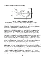
Figure.3-3 SKY77518 FUNCTIONAL BLOCK DIAGRAM
The SKY77518 is a transmit and receive front-end module (FEM) with Integrated Power
Amplifier Control (iPAC
™
) for dual-band cellular handsets comprising GSM900 and DCS1800
operation. Designed in a low profile, compact form factor, the SKY77518 offers a complete
Transmit VCO-to- Antenna and Antenna-to-Receive SAW filter solution. The FEM also supports
Class 12 General Packet Radio Service (GPRS) multi-slot operation.
The module consists of a GSM900 PA block and a DCS1800 PA block, impedance-matching
circuitry for 50
Ω
input and output impedances, TX harmonics filtering, high linearity and low
insertion loss PHEMT RF switches, diplexer and a Power Amplifier Control (PAC) block with
internal current sense resistor. A custom BiCMOS integrated circuit provides the internal PAC
function and decoder circuitry to control the RF switches. The two Heterojunction Bipolar Transistor
(HBT) PA blocks are fabricated onto a single Gallium Arsenide (GaAs) die. One PA block supports
the GSM900 band and the other PA block supports the DCS1800 band. Both PA blocks share
common power supply pads to distribute current. The output of each PA block and the outputs to
the two receive pads are connected to the antenna pad through PHEMT RF switches and a
diplexer. The GaAs die, PHEMT die, Silicon (Si) die and passive components are mounted on a
multi-layer laminate substrate. The assembly is encapsulated with plastic overmold.
Band selection and control of transmit and receive modes are performed using two external
control pads. Refer to the functional block diagram in Figure.3-2-1
below. The band select pad (BS)
selects between GSM and DCS modes of operation. The transmit enable (TX_EN) pad controls
receive or transmit mode of the respective RF switch (TX = logic 1). Proper timing between transmit
enable (TX_EN) and Analog Power Control (VRAMP) allows for high isolation between the antenna
and TXVCO while the VCO is being tuned prior to the transmit burst.
The SKY77518 is compatible with logic levels from 1.2 V to VCC for BS and TX_EN pads,
depending on the level applied to the VLOGIC pad. This feature provides additional flexibility for
the designer in the selection of FEM interface control logic.
Summary of Contents for GB130kf750
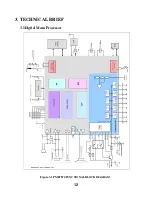
Page 12: ...12 3 TECHNICAL BRIEF 3 1Digital Main Processor Figure 3 1 PMB7890 FUNCTIONAL BLOCK DIAGRAM ...
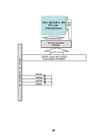
Page 28: ...28 ...
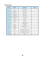
Page 29: ...29 Pin Description ...
Page 35: ...35 Circuit Diagram TP1 TP6 TP2 TP4 TP 3 TP5 ...
Page 36: ...36 Checking Flow ...
Page 37: ...37 4 2 SIM Card Trouble Test Point Circuit Diagram ...
Page 38: ...38 Checking Flow ...
Page 39: ...39 4 3 Vibrator Trouble Test Point Circuit Diagram ...
Page 40: ...40 Checking Flow NG ...
Page 41: ...41 4 4 Keypad Trouble Test Point ...
Page 42: ...42 Circuit Diagram ...
Page 43: ...43 ...
Page 44: ...44 Checking Flow ...
Page 45: ...45 4 5 RTC Trouble Test Point Circuit Diagram ...
Page 46: ...46 Checking Flow ...
Page 47: ...47 4 6 Key Backlight Trouble 4 6 1 Main Key Board LED ...
Page 48: ...48 Circuit Diagram Checking Flow ...
Page 49: ...49 4 6 2 Upper Key Board LED Circuit Diagram TP1 ...
Page 50: ...50 Checking Flow ...
Page 51: ...51 4 7 LCM Backlight Trouble Test Point Circuit Diagram ...
Page 52: ...52 Checking Flow ...
Page 53: ...53 4 8 LCM Trouble Test Point Circuit Diagram ...
Page 54: ...54 Checking Flow ...
Page 55: ...55 4 9 Microphone Trouble Test Point Circuit Diagram TP1 ...
Page 56: ...56 Checking Flow ...
Page 57: ...57 4 10 Receiver Trouble Test Point ...
Page 58: ...58 Circuit Diagram ...
Page 59: ...59 Checking Flow ...
Page 60: ...60 4 11Speaker Trouble Test Point ...
Page 61: ...61 Circuit Diagram ...
Page 62: ...62 Checking Flow ...
Page 63: ...63 4 12 Headphone Trouble Test Point Circuit Diagram ...
Page 64: ...64 ...
Page 65: ...65 Checking Flow ...
Page 66: ...66 ...
Page 67: ...67 4 13 Charging Trouble Test Point Circuit Diagram TP1 TP4 TP3 TP5 TP2 ...
Page 68: ...68 Checking Flow ...
Page 69: ...69 4 14 FM Radio Trouble Test Point ...
Page 70: ...70 Circuit Diagram ...
Page 71: ...71 Checking Flow ...
Page 72: ...72 ...
Page 74: ...74 RF Trouble TEST POINT ...
Page 76: ...76 ...
Page 77: ...77 RX Trouble TEST POINT ...
Page 78: ...78 CIRCUIT TP5 TP6 TP3 TP4 TP1 TP2 ...
Page 79: ...79 CHECKING FLOW ...
Page 80: ...80 TEST POINT CIRCUIT TP1 TP2 TP5 TP6 TP3 TP4 TP2 TP1 ...
Page 81: ...81 WAVE FORM CHECKING FLOW Replace X301 ...
Page 82: ...82 TX Trouble TEST POINT ...
Page 83: ...83 CIRCUIT WAVE FORM TP5 TP6 TP3 TP4 TP2 TP1 ...
Page 84: ...84 TEST POINT ...
Page 85: ...85 CHECKING FLOW ...
Page 86: ...86 Signal configuration CHECKING FLOW ...
Page 87: ...87 TROUBLE SHOOTING TEST POINT CIRCUIT TP5 TP6 TP3 TP4 TP1 TP2 ...
Page 88: ...88 WAVE FORM ...
Page 89: ...89 CHECKING FLOW ...
Page 90: ...90 5 DOWNLOAD 5 1 Download Setup ...
Page 100: ...100 3 DownLoad Fail If download fail that it will show red and display progress in log window ...
Page 101: ...101 Fig 2 DownLoad success DownLoad Pass will display green color ...
Page 102: ...102 6 BLOCK DIAGRAM ...
Page 103: ...103 7 CIRCUIT DIAGRMA ...
Page 104: ...104 ...
Page 105: ...105 ...
Page 106: ...106 ...
Page 107: ...107 ...
Page 108: ...108 ...
Page 109: ...109 ...
Page 110: ...110 ...
Page 111: ...111 ...
Page 112: ...112 8 BGA IC PIN Check 8 1 BGA PIN Check of MCU PMB7890 BGA use BGA non use ...
Page 113: ...113 8 2 BGA PIN Check of Memory S71GL064NA0BFW0Z0 BGA use BGA non use ...
Page 137: ...137 13 EXPLODED VIEW REPLACEMENT PART LIST 13 1 EXPLODED VIEW ...
Page 138: ...138 Ass y exploded view ...

