background image


58

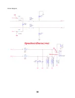
Circuit Diagram 


Summary of Contents for GB130kf750

Page 1: ...1 GB130 GB130 GB130 GB130 Service Manual Service Manual Service Manual Service Manual LG Electronics ...

Page 2: ...M Card Trouble 37 4 3 Vibrator Trouble 39 4 4 Keypad Trouble 41 4 5 RTC Trouble 45 4 6 Key Backlight Trouble 47 4 7 LCM Backlight Trouble 51 4 8 LCM Trouble 53 4 9 Microphone Trouble 55 4 10 Receiver Trouble 57 4 11 Speaker Trouble 60 4 12 Headphone Trouble 63 4 13 Charging Trouble 67 4 14 FM Radio Trouble 69 4 15 RF Trouble 73 5 DOWNLOAD 90 5 1 Download setup 90 5 2 Download Process 91 6 BLOCK DI...

Page 3: ...ot be responsible for any charges that result from such unauthorized use B Incidence of Harm If a telephone company determines that the equipment provided to customer is faulty and possibly causing harm or interruption in service to the telephone network it should disconnect telephone service until repair can be done A telephone company may temporarily disconnect service as long as repair is not d...

Page 4: ...ical equipment etc Interference from unsuppressed engines or electric motors may cause problems H Electrostatic Sensitive Devices ATTENTION Boards which contain Electrostatic Sensitive Devices ESD are indicated by the sign Following information is ESD handing Service personnel should ground themselves by using a wrist strap when exchange system boards When repairs are made to a system board they s...

Page 5: ...h Li ion inner pack 950mAh 55x34x50mm FM Receiver Yes Option 87 5 108MHz Loud Speaker Yes Memory Size TBD Will be fixed at Pre kick off Standby Time Shall support minimum test hours as hrs based on battery capacity of mAh Reference measurement conditions refer to TW 09 440 hrs 2 1mA 950mAh P P 5 Talk Time Shall support minimum test minutes as min based on battery capacity of mAh Reference measurem...

Page 6: ...clude Mute Y Ring Tone MP3 ring tone 10 Midi Y Call Alert type Ring Vibrate Ring Vibrate Ring after vibrate Silent Y Earpiece Volume 6 Level Include Mute Y Audio Mute Y GSM dual band MS 900 1800 Configuration is during software compile time Y Frequency Bands PCS dual band MS 850 1900 N A N Infrared IrDA N Bluetooth N USB N USB Mass storage N Connectivity RS232 UART Only for Phone tool download PC ...

Page 7: ...ory N Call History Call Duration Last Call time Total Call Time Y Call Waiting Y Call Swap Y Call Retrieve Y Auto Answer Not supported in Headset Mode Y Auto Redial Y Calling Line Y Full Call Divert Y Speed Dialing Y Last Number Redial Y Multi Party Call Y Call Management ECT Explicit Call Transfer 4 Send N Automatic Network Selection Y Manual Network Y Preferred Network Y Network Network Service ...

Page 8: ...SIM or Phone Multi Delete Y CFU Call Forwarding Unconditional Y CFB Call Forwarding on Mobile Subscriber Busy Y CFNRy Call Forwarding on No Reply Y CFNRc Call Forwarding on Mobile Subscriber Not Reachable Y BAOC Barring of All Outgoing Calls Y BOIC Barring of Outgoing International Calls Y BOICexHC Barring of Outgoing International Calls except those directed to the Home PLMN Country Y BAIC Barrin...

Page 9: ...sage Y Forward Message Y Extract Number from Message Y Message Status Y Message Unread Y Settable Message Center Number Reply Path and Validity Y Visible and Audible Message Receive Y No for Audible Voice Mail Y Settable Voice Mail Center Number Y Message Protocol Normal Fax National Paging X400 ERMES Voice Y Message Overflow Indicator Y Message Center Number Y Short Message Nokia Smart Message N ...

Page 10: ...ecords 18 chars Y To Do N Scheduler Memo MAX 10 records 80 chars Y Setting Local Time Y Display Two Number of Cities Time Dual Clock N Daylight saving N World Time NITZ Y Unit converter Length Weight Volume Surface Velocity Temperature User defined Y Stop Watch Y Calculator Y Phone Book Sync Only For service Center TBD PC Sync Message Sync TBD Game 1 game SUDOKU TBD Y Emergency Call Y Handset Lock...

Page 11: ...ime Zone Y Daylight saving Y Alarm Manager Y Dimming Clock N Power off Alarm Y Real Time Clock On Alarm Event Y Mobile Tracking software For India Asia TBD Others M DOG For China TBD Accessory microSD Adapter N Mono earmic without hook switch Y ...

Page 12: ...12 3 TECHNICAL BRIEF 3 1Digital Main Processor Figure 3 1 PMB7890 FUNCTIONAL BLOCK DIAGRAM ...

Page 13: ...ery connection hence eliminating the need for an external Power Management Unit The X GOLDTM102 has different power down modes and an integrated power up sequencer The X GOLDTM102 is powered by the C166 S V2 MCU and TEAKLite DSP cores The operating temperature range from 30 C to 85 C It is manufactured using the 0 13 μm CMOS process 3 1 2 Features Baseband High performance fixed point TEAKlite DSP...

Page 14: ...Fully digital controlled crystal oscillator core with a highly linear tuning characteristic Mixed Signal and Power Management Unit DC DC boost for voltages up to 15 V for driving White or Blue LEDs 8 Ohm loud speaker driver 250 350 mW 16 Ohm earpiece driver 32 Ohm headset driver Measurement interfaces PA temperature battery voltage battery temperature and ambient temperature Accessory Detection PC...

Page 15: ...ated voice signal passes through a digital voiceband filter The resulting 4 Mbit s data stream is D to A converted by a multi bit oversampling converter postfiltered and then amplified by a programmable gain stage The output buffer can drive a handset ear piece or an external audio amplifier an additional output driver for external loud speaker is implemented In the transmit direction the differen...

Page 16: ...es are suspended and then resumed automatically after the call or SMS session has ended 3 1 5 Bus Concept The X GOLDTM102 has two cores a microcontroller and a DSP each with its own bus There is an Shared memory interconnection between the TEAKlite bus and the C166S V2 X Bus C166S V2 Buses The C166S V2 is connected to four buses 1 IMB Internal Program bus 2 DPMI Data Program Bus 3 X Bus 4 PD Bus T...

Page 17: ...ardware timer Charger idle voltages up to 20 V can be handled An integrated overvoltage protection protects batteries and system against overvoltage White blue backlight generation is supported with a special driver for very a low external parts count Power consumption during operation phases is minimized due to flexible clock switching In the Standby Mode most parts of the device are switched off...

Page 18: ...ecryption keystream It implements the following algorithms A5 1 A5 2 and A5 3 3 1 11 Asynchronous Operation Mode Concept The X GOLDTM102 can operate in either The traditional synchronous mode with the 26 MHz system clock synchronized on the base station A special asynchronous mode XO concept In the asynchronous mode the 26 MHz clock input is not synchronized with the base station the residual freq...

Page 19: ...S71GL128N _ 105 ns access time S71GL512N _ 25 ns page read times _ Packages 12 0 x 9 0 mm x 1 2 mm FBGA TLD084 S71GL512N 11 6 x 8 0 mm x 1 2 mm FBGA TLA084 S71GL128N _ Operating Temperature 25 C to 85 C Wireless General Description The S71GL Series is a product line of stacked Multi chip Product MCP packages and consists of _ One Flash memory die _ One pSRAM ...

Page 20: ... PA block supports the GSM900 band and the other PA block supports the DCS1800 band Both PA blocks share common power supply pads to distribute current The output of each PA block and the outputs to the two receive pads are connected to the antenna pad through PHEMT RF switches and a diplexer The GaAs die PHEMT die Silicon Si die and passive components are mounted on a multi layer laminate substra...

Page 21: ...attenuation Low amplitute ripple Impedance transformation from 50 W to 150 W for both filters Suitable for GPRS class 1 to 12 Features Package size 2 0 x1 6 x 0 68 mm3 Package code QCS10H RoHS compatible Approx weight 0 008 g Package for Surface Mount Technology SMT Ni gold plated terminals Electrostatic Sensitive Device ESD Pin configuration 1 Input Filter 1 4 Input Filter 2 6 7 Output balanced F...

Page 22: ...gned for Wireless Handsets PDAs and other mobile devices Compatible with Low Power 1 8V Logic I O Threshold control signals DESCRIPTION The TPA6202A1 is a 1 25 W mono fully differential amplifier designed to drive a speaker with at least 8 Ώ impedance while consuming less than 37 mm2 ZQV package option total printed circuit board PCB area in most applications This device operates from 2 5 V to 5 5...

Page 23: ...ogrammable charge currents 85mA to 1A programmable battery full threshold thermal protection battery temperature monitoring reverse current blocking and trickle charge The device also provides AC adapter power good and charge status indications to the system MP26021 is available in a 10 pin 3mm x 3mm QFN package FEATURES Input Surge Up to 28V Adapter or USB Input Programmable Charge Current 85mA t...

Page 24: ...t Protection AC Adapter Power Good Indicator Charge Status Indicator Programmable Soft Start Programmable Charge Termination Current Threshold Tiny 10 Pin QFN 3mm x 3mm Package APPLICATIONS Cell Phones MP3 Players Smart Phones PDAs Digital Cameras ...

Page 25: ...and one external bypass capacitor The device offers significant programmability catering to the subjective nature of FM listeners audio preferences and variable FM broadcast environments worldwide The Si4709 incorporates a digital processor for the European Radio Data System RDS and the US Radio Broadcast Data System RBDS including all required symbol decoding block synchronization error detection...

Page 26: ...h an integrated regulator allowing direct connection to a 2 7 to 5 5 V battery for VD and 2 7 to 5 5 V battery for VA The Si4708 09 device s high level of integration and complete FM system production testing increases quality to manufacturers improves device yields and simplifies device manufacturing and final testing ...

Page 27: ...ed into Red Green and Blue sub pixels and dots which are arranged in vertical stripes Main LCD color is determined with 262 144 colors signal for each pixel The IM200BBN2A has been designed to apply the interface method that enables low power high speed and high contrast The IM200BBN2A is intended to support applications where thin thickness wide viewing angle and low power are critical factors an...

Page 28: ...28 ...

Page 29: ...29 Pin Description ...

Page 30: ...IM Card Interface Figure 3 9 SIM CARD Interface Signals Description SIM_RST This signal makes SIM card to HW default status SIM_ CLK This signal is transferred to SIM card SIM_I O This signal is interface datum ...

Page 31: ...31 3 10 KEYPAD Interface Figure 3 10 KEY PAD Interface The keypad is a 4x6 scan matrix 4 input and 6 output pins ...

Page 32: ...32 3 11 Key LED Interface Figure 3 11 Key LED Interface This handset has 8 LEDs that illuminates blue color Control signal is controlled byX Gold102 with PWM and handset has 3 methods ON OFF Dimming ...

Page 33: ...33 3 12 Vibrator Interface Figure 3 12Vibrator Interface This handset has Vibrator operation Control signal is controlled by X Gold102 ...

Page 34: ...ting 4 1 Power On Trouble Test Point Check Points Battery Voltage Need to over 3 35V Power On key detection PWRON signal Outputs of LDOs U301 EGV Voltage PART VBUF 2 8V TP1 VMEM 2 85V TP2 VIO 2 85V TP3 VSIM 2 85V TP4 VRTC 1 5V TP5 VANA 2 5V TP6 ...

Page 35: ...35 Circuit Diagram TP1 TP6 TP2 TP4 TP 3 TP5 ...

Page 36: ...36 Checking Flow ...

Page 37: ...37 4 2 SIM Card Trouble Test Point Circuit Diagram ...

Page 38: ...38 Checking Flow ...

Page 39: ...39 4 3 Vibrator Trouble Test Point Circuit Diagram ...

Page 40: ...40 Checking Flow NG ...

Page 41: ...41 4 4 Keypad Trouble Test Point ...

Page 42: ...42 Circuit Diagram ...

Page 43: ...43 ...

Page 44: ...44 Checking Flow ...

Page 45: ...45 4 5 RTC Trouble Test Point Circuit Diagram ...

Page 46: ...46 Checking Flow ...

Page 47: ...47 4 6 Key Backlight Trouble 4 6 1 Main Key Board LED ...

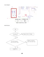
Page 48: ...48 Circuit Diagram Checking Flow ...

Page 49: ...49 4 6 2 Upper Key Board LED Circuit Diagram TP1 ...

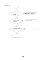
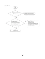
Page 50: ...50 Checking Flow ...

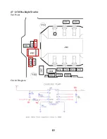
Page 51: ...51 4 7 LCM Backlight Trouble Test Point Circuit Diagram ...

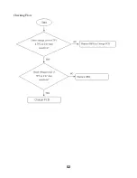
Page 52: ...52 Checking Flow ...

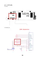
Page 53: ...53 4 8 LCM Trouble Test Point Circuit Diagram ...

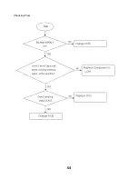
Page 54: ...54 Checking Flow ...

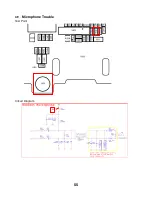
Page 55: ...55 4 9 Microphone Trouble Test Point Circuit Diagram TP1 ...

Page 56: ...56 Checking Flow ...

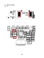
Page 57: ...57 4 10 Receiver Trouble Test Point ...

Page 58: ...58 Circuit Diagram ...

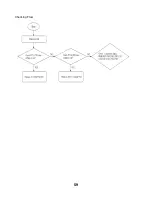
Page 59: ...59 Checking Flow ...

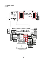
Page 60: ...60 4 11Speaker Trouble Test Point ...

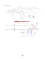
Page 61: ...61 Circuit Diagram ...

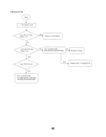
Page 62: ...62 Checking Flow ...

Page 63: ...63 4 12 Headphone Trouble Test Point Circuit Diagram ...

Page 64: ...64 ...

Page 65: ...65 Checking Flow ...

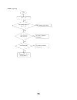
Page 66: ...66 ...

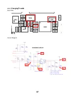
Page 67: ...67 4 13 Charging Trouble Test Point Circuit Diagram TP1 TP4 TP3 TP5 TP2 ...

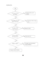
Page 68: ...68 Checking Flow ...

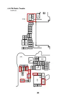
Page 69: ...69 4 14 FM Radio Trouble Test Point ...

Page 70: ...70 Circuit Diagram ...

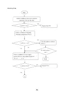
Page 71: ...71 Checking Flow ...

Page 72: ...72 ...

Page 73: ...73 4 15 RF Trouble SHOOTING REFERENCE PART Description U101 PAM Power Amp Module ASM X301 DCXO 26MHz W101 Mobile Switch U102 RX SAW Filter ...

Page 74: ...74 RF Trouble TEST POINT ...

Page 75: ... FLOW Check RF output power form PA in U101 An analog signal pass through PAM Matching components SW W101 Antenna Matching components and Antenna contact point Then finally pass it on to main Antenna RF output power in AT101 AT102 ...

Page 76: ...76 ...

Page 77: ...77 RX Trouble TEST POINT ...

Page 78: ...78 CIRCUIT TP5 TP6 TP3 TP4 TP1 TP2 ...

Page 79: ...79 CHECKING FLOW ...

Page 80: ...80 TEST POINT CIRCUIT TP1 TP2 TP5 TP6 TP3 TP4 TP2 TP1 ...

Page 81: ...81 WAVE FORM CHECKING FLOW Replace X301 ...

Page 82: ...82 TX Trouble TEST POINT ...

Page 83: ...83 CIRCUIT WAVE FORM TP5 TP6 TP3 TP4 TP2 TP1 ...

Page 84: ...84 TEST POINT ...

Page 85: ...85 CHECKING FLOW ...

Page 86: ...86 Signal configuration CHECKING FLOW ...

Page 87: ...87 TROUBLE SHOOTING TEST POINT CIRCUIT TP5 TP6 TP3 TP4 TP1 TP2 ...

Page 88: ...88 WAVE FORM ...

Page 89: ...89 CHECKING FLOW ...

Page 90: ...90 5 DOWNLOAD 5 1 Download Setup ...

Page 91: ...wnload tool 1 Installation Installing this program before you must install Prolific USB to Serial Comm Port driver first Install SetupDWForService msi when driver installing is Okay Click Next button to continue ...

Page 92: ...92 Choose a item of what you want Click Next button to continue Make sure of setup is correct Click Next Button to Start installing ...

Page 93: ...93 Installation finish Click Close button to finish If you want to remove this software please go to Console and choose add remove Install to remove DWForService ...

Page 94: ...94 It will present a shortcut in the desktop after installing finish This is DWForService download software ...

Page 95: ...tware Description as follows 1 Choose PCBA item is for Reformat the PCBA with Calibration Choose MMI item only is for Upgrade customization SW no need to calibration If you want change it please modify C Program Files DownLoad DWForService LGDownLoad ini Station 2 1 is PCBA D L 2 is MMI D L ...

Page 96: ...RF EEP Area PCBA bin file will over write Security RF EEP Area If you only choose Search Dir it will to use fls eep dffs cust files Example This example is choose GB110 00 V10g 404 XX FEB 10 2009_BIN to download Click the button with red mark then present below picture Find the software with GB110 00 V10g 404 XX FEB 10 2009_BIN ...

Page 97: ...97 Choose the GB110 00 V10g 404 XX FEB 10 2009_BIN and then click the button with red mark 4 Choose Comport number 5 Click RUN button to execute ...

Page 98: ...98 3 Download flow 1 Start Download Will present download window after make sure of setting no error When appear above picture Will automatic execute download program after DUT open power ...

Page 99: ...99 2 Downloading Download program will according to software download Every software will display in List ...

Page 100: ...100 3 DownLoad Fail If download fail that it will show red and display progress in log window ...

Page 101: ...101 Fig 2 DownLoad success DownLoad Pass will display green color ...

Page 102: ...102 6 BLOCK DIAGRAM ...

Page 103: ...103 7 CIRCUIT DIAGRMA ...

Page 104: ...104 ...

Page 105: ...105 ...

Page 106: ...106 ...

Page 107: ...107 ...

Page 108: ...108 ...

Page 109: ...109 ...

Page 110: ...110 ...

Page 111: ...111 ...

Page 112: ...112 8 BGA IC PIN Check 8 1 BGA PIN Check of MCU PMB7890 BGA use BGA non use ...

Page 113: ...113 8 2 BGA PIN Check of Memory S71GL064NA0BFW0Z0 BGA use BGA non use ...

Page 114: ...PAM SKY77518 No TX No RX U301 BB chipset PMB7880 No power on No service etc X302 32 768KHz Crystal No Booting X301 26MHz Crystal No TX No RX J601 Up board connector LCM no display Keypad not working U901 FM radio No FM U803 Charging IC No Charging ...

Page 115: ...15 J801 Battery Connector No Charging J702 SIM connector No SIM J701 I O Connector No Charging etc J802 Vibrator connector No Vibrator U501 Speaker AMP No Speaker J603 Keypad connector Keypad not working ...

Page 116: ...Engineering Mode 1 Function Test 1 1 Test Purpose To verify handset functional is pass or fail when assembled by visual check 1 2 Test Facilities List 1 LCD 2 Earphone 3 Vibrator 4 GSM tester 5 FM transmitter ...

Page 117: ...d LED 3 Vibrator Vibrator function check Always on All keys function check Method 1 screen shows all icons one by one then it disappear in screen Method 2 screen shows icon of press it as phone instruction 4 Keyboard Speaker Speaker check 5 Audio Mic_ Receiver loop Main Mic to Main Receiver audio loop check 6 Headsets Earpiece Aux Mic to Aux Receiver audio loop check 7 Melody Speaker and Melody fu...

Page 118: ...t setup 11 2 APT Technologies calibration tool 11 2 1 Installation Before install this program it must install GPIB VISA drivers and Net Framework 2 0 at first Press the next to continue the installation Fig 3 APT Technologies installation ...

Page 119: ...on Only Agilent 8960 is the only available for selection at present CMU200 has no function Fig 4 Choose the wireless communication test set type Choose the installing catalogue if it is necessary you can change the folder to install Press next to continue the installation Fig 5 Choose the catalogue to install ...

Page 120: ...on Only Agilent 8960 is the only available for selection at present CMU200 has no function Fig 6 Choose the wireless communication test set type Choose the installing catalogue if it is necessary you can change the folder to install Press next to continue the installation Fig 7 Choose the catalogue to install ...

Page 121: ...s back to set up Fig 8 Confirm installing While installing it will appear a window like Fig 9 it will begin to install the test scripts after choosing installation if change the catalogue of installing before this installation catalogue must keep the same with APT Fig 9 Installation Test Script ...

Page 122: ...es finally pushing and closing the button finishes installing Fig 10 It finishes to install It will present two shortcuts in the tabletop after finishing the installation ATP Tools Icon Auto Cable Loss Compensation Tools Icon ...

Page 123: ... 8 7 2 Script file File of test script show the testing script file location and file name 3 FT It will select the script for Final Test 4 Cal It will select the script for Calibration 5 COM Show the communication port connected with mobile phone at present 6 List The large window on the right shows the tests list at present 7 Progress Bar Show that the test progress at present 8 Serial Number Sam...

Page 124: ... test 13 Quit Close the APT program 14 Pass Count the quantity of Pass at present if reopens the program it will calculate again 15 Total Count and quantity of test at present if reopens the program it will calculate again 16 Result Show the test result at present 17 Error It will show the fist fail message 18 The state bar 1 Total Count the quantity of test at present 2 Fail Count Fail quantity a...

Page 125: ...to test After opening the program confirms that it is errorless to set up some lower Start will appear the Bar Code input window such as Fig 12 begin to test like Fig 13 after scanning or inputting Bar Code Fig 12 Input Bar Code window ...

Page 126: ...y test the procedure serial number 2 Sub Test the procedure serial number less importantly 3 Description It is tested that the procedure proves 4 P F P means test succeeds F means test failure 5 MV Number value received in test 6 Unit Unit 7 Output Line Word bunch got in test 8 LL The lower limits 9 UL The upper limits 10 Test Time This tests the execution time of procedure ...

Page 127: ...the result in Result if there is Error Message will show on Error Window with Bar Code input will jump out for continue test the next mobile If input QUIT it can close the input Bar Code window and can make fix or change and test the script Fig 14 Sketch map that test fails ...

Page 128: ...Pass will getting green and jump out the input Bar Code window for next test If input QUIT it can close the input Bar Code window and can make fix or change and test the script Fig 15 Test succeeds in finishing the sketch map ...

Page 129: ...129 11 2 4 Set up Double click the Arima icon will show set up window Fig 16 Double click ARIMA icon window ...

Page 130: ... Choose default test item 2 Power Supply Power Supply Type Type of power supply 0 663xx Power Supply Address Power supply GPIB address 3 COM Port Com Port The communication port with mobile phone Baud Rate Baud Rate with the mobile phone communication 115200 DTR DTR with the mobile phone communication 0 RST RST with the mobile phone communication 1 Platform ulc2 or ulc2 xmm1020 Prefix Mobile phone...

Page 131: ...k for Self Type Choose to carry out the type to test script at present 5 DUMY IMEI No Function DUMY IMEI Establishment should store the number of IMEI Label 6 Debug If selected it will continuous the test however test item is fail After set up and finish the above six item push save button will appear a window click yes to store and initialize Click Exit to close config setting window Fig 18 Store...

Page 132: ...The picture is as follows after opening Fig 19 Auto Cable Loss Compensation This procedure and APT are very much the same more different place among them must choose the type of Golden first on the left and input and test the number of times Times the most largely The procedure will judge automatically if each loss value is less than 0 1 to finish automatically if exceed testing the figure does no...

Page 133: ...133 12 Stand alone test 12 1 Test program setting 12 1 1 Set COM port 12 1 2 Check PC Baud rate 115200 12 1 3 Confirm EEPROM Delta file prefix name ...

Page 134: ...d then Update Info for communicating Phone and Test Program 12 1 5 For the purpose of the Stand alone Test Change the phone to ptest mode and then click the Reset bar 12 1 6 Select Non signaling in the Quick Bar menu Then Stand alone Test set up finished ...

Page 135: ...ling mode bar and then confirm OK test in the command line 12 2 2 Put the number of TX channel in the ARFCN 12 2 3 Select TX in the RF mode menu and PCL in PA level menu 12 2 4 Finally Click Write All bar and try the efficiency test of phone ...

Page 136: ...136 12 3 RX Test 12 3 1 Put the number of RX channel in the ARFCN 12 2 2 Select RX in the RF mode menu 12 2 3 Finally Click Write All bar and try the efficiency test of phone ...

Page 137: ...137 13 EXPLODED VIEW REPLACEMENT PART LIST 13 1 EXPLODED VIEW ...

Page 138: ...138 Ass y exploded view ...

Page 139: ...5901 1 2 Screw 409 00000 0083 Machine Screw_Flat_Cross JCIS _1 4mm_1 2mm_SILVER_Steel_ Plating Zinc_KUAOLENG SHANGHAI _Nylok GMZZ0029101 4 2 Screw 409 00000 0082 Machine Screw_Flat_Cross JCIS _1 6mm_3mm_BLACK_Steel_Pl ating Zinc_KUAOLENG SHANGHAI _Nylok GMZZ0029001 6 2 Screw cap 405 71330 0005 Cover_7133_SILVER_RUBBER SILICON RUBBER_Painting_Screw cap_YIDA KUNSHAN _N A MCCH0153001 2 2 Key 404 7133...

Page 140: ...MORY_S71GL064NA0BFW0Z0_FPBGA_56 BAL LS_64M 16M_SPANSION_FLASH PSRAM EUSY0384101 1 5 U403 311 0000 00675 I C STANDARD LOGIC_NC7SZ08P5X_SC70_5 PINS_NoMemory_ FAIRCHILD_2 INPUT AND GATE EUSY0384401 1 5 U501 311 0000 00689 I C AUDIO POWER AMPLIFIER_TPA6202A1ZQVR_BGA_8 Balls_ NoMemory_TI_Vo 3 6V 0 63 W 8 Ohm EUSY0376801 1 5 U502 311 0000 00676 I C STEREO AUDIO POWER AMPLIFIER_TS486 IQT_DFN_8 PIN S_NoMe...

Page 141: ...ator Coin Type Without Connector_C1030L 070022302 2408_ Φ10 0 3 00mm_LNLON_Wire type SJMY0009701 1 3 Antenna 330 0000 00127 ANTENNA EMBEDDED_7133_DUAL BAND GSM DCS _SILVER_ NC028IA84_SHANGHAI UNIVERSE_PC Carrier Metal ANT SNGF0049501 1 3 Keypad Board 8 05 7133N0 01 Keypad Board Ass y_7133_NATURAL_7133 KB SAEE0035001 1 5 BAT101 306 0000 00033 Li Button Battery Cell RTC Reflowable_3 3V_0 015mAh_NoCo...

Reviews: