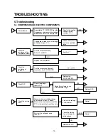
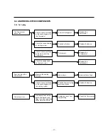
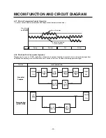
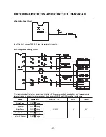
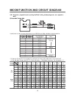
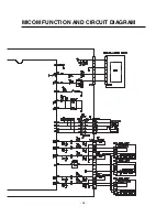
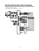


6-2-9. Communication Circuit between MAIN PCB and DISPLAY PCB
Communication circuit for an information exchange between MAIN MICOM and DISPLAY PCB in MAIN PCB
If there is an interruption in information exchange between MAIN MICOM and DISPLAY PCB in MAIN PCB for more than 30
seconds, it causes a communication malfunction.
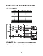
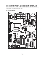
MICOM FUNCTION AND CIRCUIT DIAGRAM
- 29 -
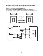
DISPLAYPCB
MAIN PCB
MAIN MICOM
DC 12V
GND
Transmitting (Error)
Receiving (NOTCH)
LCD Controlling
MICOM
Summary of Contents for GC-W061 series
Page 8: ... 8 3 Exterior 3 1 Exterior GC W061 EXTERIOR ...
Page 9: ...GC W101 EXTERIOR 9 ...
Page 10: ...EXTERIOR 10 ...
Page 11: ...GC W141 EXTERIOR 11 ...
Page 12: ...EXTERIOR 12 ...
Page 14: ...CIRCUIT DIAGRAM 14 GC W101 GC W141 ...
Page 32: ...6 4 2 Replacement Parts List MICOM FUNCTION AND CIRCUIT DIAGRAM 32 ...
Page 33: ...6 4 3 PWB ASS Y DISPLAY AND PARTS LIST MICOM FUNCTION AND CIRCUIT DIAGRAM 33 ...
Page 35: ...MICOM FUNCTION AND CIRCUIT DIAGRAM 35 ...