background image

7. Organization of the PCA, PMA and Lead-in Area

1) Layout of CD-ROM disc

16

Center hole

Clamping and Label Area

Information Area

Lead-in Area

Lead-in Area

Diameter 15 mm

Diameter 46 mm

Diameter 120 mm

Program Area

Read Only Disc

Lead-out Area

Program Area

Lead-out Area

Center hole Clamping and Label Area

Information Area

PCA PMA

Test Area

Count Area

Diameter 15 mm

Diameter 45 mm

Diameter 120 mm

Unrecorded Disc

Tsl-00:35:65 Tsl-00:15:05 Tsl-00:13:25

Tsl

99:59:74
00:00:00

in

out

Test Area : for performing OPC procedures.

Count Area : to find the usable area immediately in T.A

Tsl : start time of the Lead-in Area, as encoded in ATIP

PMA : Program Memory Area

Disc Center

Disc Center

2) Layout of CD-R/RW disc

Summary of Contents for GCC-4241N

Page 1: ...Slim CD RW DVD ROM Drive SERVICE MANUAL MODEL GCC 4241N P NO 3828HS1043A August 2003 Printed in Korea MODEL GCC 4241N website http biz LGEservice com e mail http www LGEservice com techsup html ...

Page 2: ...d Lead in Area 16 8 Function of PCA and PMA area 17 9 OPC and ROPC 17 10 Writing Process of DISC 18 DESCRIPTION OF DATA PROCESSING 19 22 1 Data Processing Flow 19 2 Copy Protection and Regional Code Management Block 20 3 About Prevention the DVD ROM from to be copy 21 4 About the DVD ROM Regional Code 22 INTERNAL STRUCTURE OF THE PICK UP 23 24 1 Inner Circuit of the PICK UP 23 2 Signal detection o...

Page 3: ...V 10 16xPCAV 24x Max CAV 3 Read speed CD R RW ROM 24x 24x 24x Max CAV CD DA DAE 20x Max CAV DVD R RW ROM 4x 4x 8x Max CAV DVD Video CSS 4x Max CAV DVD RAM 2 6G 4 7G 2x ZCLV 4 Sustained Transfer rate CD ROM 3 600 kB s 24x Max DVD ROM 11 08 Mbytes s 8x Max 5 Burst Transfer rate Ultra DMA Mode2 DMA MW Mode2 PIO Mode4 6 Support CD TEXT read write 5 Audio 1 Outputs 16 bit digital data over ATA interfac...

Page 4: ...io Mixed Mode Audio and Data Combined CD I Video CD CD Plus CD Extra CD Text Applied Format depend on Authoring Tool Writing Method Disc at once DAO Session at once SAO Track at once TAO Variable packet writing Fixed packet writing Multi session Embedded Running OPC Buffer Under run Prevention 4 Cache memory 2 MB 5 Disc diameter 120 mm 80mm 6 Data capacity User Data Block DVD ROM Book A B 2 048 by...

Page 5: ...xCLV 10 16PCAV 24xMAX CAV CD RW Normal Disc 4xCLV High speed Disc 4x 10xCLV Ultra speed Disc 10xCLV 10 16xPCAV 24xMAX CAV Rotational Speed CD R RW 4xCLV Approx 800 2 020 r min 10xCLV Approx 2 000 5050 r min 24xMAX CAV Approx 4 860 5 200 r min 2 Data Transfer Rate Sustained Transfer Rate Read DVD ROM Single Layer 11 08 Mbytes s 8x Max Dual Layer 11 08 Mbytes s 8x Max DVD R 3 95GB 5 54 Mbytes s 4x M...

Page 6: ...ing time Assumption Used in a normal office environment 6 Power Requirements 1 Source Voltage 5V 5 Ripple Less than 100mVp p 2 Current Stand By Sleep 22 mA typical OS Windows XP Continuous Read 660 mA typical CD 24x Max CAV 540 mA typical DVD 8x Max CAV Continuous Write 800 mA typical CD R 24x Write Seek 1 0A typical 1 5A Max 24x Max CAV Spin UP Spindle motor start up 1 0A typical 1 8A Max 24x Max...

Page 7: ...NEL A Remove the Front Panel The Front Panel is a snap on type B At this time be careful not to damage the 3 hooks a of the it See fig 3 C Release 3 screws C and remove the Cover Bottom 3 4 BASE PICK UP A Remove the FPC Cable At this time the FPC connector must be pulled in the direction of Front carefully B Remove the Base Pick up 4 1 A A A B B B 2 4 2 3 C C C CABINET 2 HOOKS HOOKS a FRONT PANEL ...

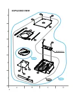
Page 8: ...8 PBM00 MAIN C B A A B C D 1 2 3 4 5 450 450 450 001 012 011 013 451 451 451 450 450 005 004 003 A02 A00 A01 EXPLODED VIEW ...

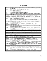
Page 9: ...hanged conditions of disc and change in operating temperature Jitter The 16 value of the time variation between leading and trailing edges of a specific I3 I11 pit or land as measured by Time Interval Analysis Deviation The difference between a fixed value of Pit length and Land length TOC Table Of Contents in the Lead in Area the subcode Q channel contains information about the Tracks on the disc...

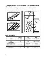
Page 10: ...Land Track pitch p Radial Direction Iw A O a a Groove Land Radial Error Signal The Groove wobble Average center Actual center CD ROM CD R CD RW Standard Yellow Book Orange Book II Orange Book III Record Not available Write once Re writable I 11 Itop 0 6 0 6 0 55 M11 0 70 HF Modulation Write Laser Power mW 10 30 mW 6 25 mW Read Laser Power mW 0 5 mW 0 7 mW 1 0 mW Jitter 35 nsec 35 nsec 35 nsec Refl...

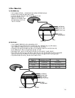
Page 11: ...n the disc It is so called WORM Write Once Read Many CD It is composed of polycarbonate layer Organic dye layer Reflective layer and Protective layer Gold Silver Reflective layer is used to enhance the reflectivity According to the kinds of Organic dye layer it is divided by Green CD Gold CD Blue CD Laser Wavelength 780 nm Laser Power read 0 7 mW Recording Power 4x 10 15mW 8x 14 20mW 12x 15 30mW 1...

Page 12: ... reading is enabled by the difference of reflectivity It is possible to overwrite about 1000 times Laser Wavelength 780 nm Laser Power Read 1 0mW Recording Power Erase 4 18mW Write 6 45mW When disc rewriting new data is overwritten previously recorded data Polycarbonate layer has a Pre Groove which make a track Lens H D Beam Spot Focusing Lens Laser Spot at Constant Read Intensity Reflected Light ...

Page 13: ...Spot Recorded Mark Reflected Light Signal Reflected Light Signal Below ORP Mark Too Short At Optimum Record Power ORP Above ORP Mark Too Long Time 6 Writing process of CD RW Disc Write Power Erase Power Read Power Groove Crystal Amorphous Amorphous Recorded state lower reflectivity Melting quenching Heating gradual cooling Crystal phase Erased state higher reflectivity ...

Page 14: ...Area Lead out Area Center hole Clamping and Label Area Information Area PCA PMA Test Area Count Area Diameter 15 mm Diameter 45 mm Diameter 120 mm Unrecorded Disc Tsl 00 35 65 Tsl 00 15 05 Tsl 00 13 25 Tsl 99 59 74 00 00 00 in out Test Area for performing OPC procedures Count Area to find the usable area immediately in T A Tsl start time of the Lead in Area as encoded in ATIP PMA Program Memory Ar...

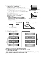
Page 15: ...ad_In area so that general Driver can read it Because PCA and PMA area exist before Lead In area General CD Player or CD ROM Drive can t read these areas 9 OPC and ROPC 1 OPC Optimum Power Control This is the first step of writing process because CD writer has its own laser power value and media have different writing characteristics This is determined by the Writing characteristic speed temperatu...

Page 16: ...lose Reference B level value c Normalization of B level is used to eliminate the effect of reflectivity fluctuation The reflected B level value is normalized by the disc reflectivity itself 18 CD R RW Media Write Strategy Determination PCA Test Area Program Area PMA Area Lead In Area Lead out Area OPC PCA Count Area ROPC Recording Capacity of CD R RW 74Minute Recording media 2048 Byte Sector X 75 ...

Page 17: ...ice EFM demodulator CiRC error correction Audio DAC C3 decoder Buffer Memory controller CSS controller Atapi interface control Data PLL Servo ADC Focus tracking control output Sled control output CAV Spindle control P up Unit IC101 AN22107A RF AMP CD DVD IC201 MN103S63G TE CSO GEN FE GEN FLASH ROM DRAM IC602 IC601 DRAM ...

Page 18: ...e regional code and plays title in the case of allowed regional code only 2 Management of DVD Disc for the scrambled of data 1 DVD ROM and DVD player of host generate the KEY 1 respectively transfer to opposite part the KEY 2 is received recognizes the data transfer or not with this value and generates the bus key encoded the data 2 Encoded Disc Key and Title Key host is transfer with the bus Key ...

Page 19: ...decoder generates the challenge key 10 Byte and transfers to drive The board and drive generate key 1 5Byte with the challenge key respectively Of course the Algorithm generating the key 1 is not known 3 Compare with the generated key 1 if it corresponds each other the first step of authentication is completed This is a course to identify the MPEG 2 decoder with a drive 4 The second step of authen...

Page 20: ...M PLW PNG NZL AUS 4 The disc has the regional code of 8 bit Example The disc manufactured in the U S A has the number one Transfer to MPEG 2 decoder reading the regional code If the board is setting to the regional code 1 for the U S A Check the received regional code to number 1 all or not transfer the data to VGA card in accordance with only a case among the three case Regional code Receiving da...

Page 21: ...INTERNAL STRUCTURE OF THE PICK UP 1 Inner Circuit of the PICK UP HOP 6061T 23 operating ...

Page 22: ...ethod A D B C k x F H E G This signal is generated in RF IC IC101 AN22107A and controls the pick up s left and right shift to find to track on Disc 3 RF Signal A B C D This signal is converted to DATA signal in DSP IC IC201 MN103S63G 24 Pick Up module Photo Diode Tracking Focusing Infrared Iaser k F H E G A D B C A D B C k F H E G Offset TE Tp Sub2 Main Tp 2 Sub1 Track Center F E D C A B H G ...

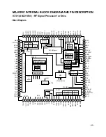
Page 23: ...2 10 VHALF 11 VR06 12 LPC1 13 LPC0 14 EDRV 15 FPDMN 16 FPDMP 17 GND3 18 RDRVN2 19 RDRVN1 20 RDRV 21 RREFDET 22 WDRVN2 23 WDRVN1 24 WDRV 25 WREFDET 76 WBL 50 NC2 49 VCC5 48 BMC 47 PKC 46 RFENV 45 CDEFECT 44 GND2 41 OFTR 40 BDO 39 VDD 38 NC1 37 SCK 36 SEN 35 STDIO 34 TOK 33 XWTGT 32 ADCLR 31 ADCK 30 VSS 29 XSTANBY 28 VFOSHORT RAPC 27 WAPC 26 VCC3 43 ROPCSH2 DTRD 42 ROPCSH1 IDGT 77 SCFCLK 78 NC4 79 W...

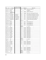
Page 24: ...41 OFTR O OFTR TC output 42 ROPCSH1 I ROPC1 sample hold timing input IDGT 43 ROPCSH2 I ROPC2 sample hold timing input DTRD 44 GND2 PS GND for RF 5V 45 CDEFECT DEFECT envelope detection filter 46 RFENV O RF envelope output 47 PKC MSC Peak envelope detection filter 48 BMC MSC Bottom envelope detection filter No Name I O Funtion 49 VCC5 PS Power supply CMOS I F 3 3V 50 NC2 Non connection 51 DFLTOP O ...

Page 25: ...f w and 8 Kbyte microcode and 2 Mbit DRAM 32 bit CPU core BCU DRAMC DMA 1 Mbit DRAM OnChip Debug Data memory 6 Kbyte f w 4 Kbyte microcode Instruction memory 128 Kbytes CGEN MODE WDT 16 bit timerx6 f w timerx2 microcode SYSTEM I F INTC General purpose I O Serial interface HOST I F MPEG I F ECC DMA I F ATAPI General purpose I O bus SERVO IO Core1 IO SERVO core Core2 RAM CIRC DVD ROM Formatter CD PR...

Page 26: ...55 RVI FADR15 27 28 165 154 VHALF DRAMVDD15 28 29 164 153 NARF VOUT 29 30 163 152 ARF DRAMVDD33 30 31 162 151 AVSSB DRAMVSS 31 32 161 150 PLFLT1 _VSS NC 33 160 149 PLFLT2 TxD 32 34 159 148 AVSSC SCLOCK 33 35 158 147 RFDIF NRST 34 36 157 146 CSLFLT SDATA 35 37 156 145 WBLIN RxD 36 38 155 144 AVDDC P2 37 39 154 143 TRCRS P3 38 40 153 142 VCOF P4 39 41 152 141 AVDDD P5 40 42 151 140 LOUT P6 41 43 150...

Page 27: ...ut to general purpose port flash 16 16 N1 P8 FADR18 CPUADR17 I I O Flash Address output to general purpose port flash 17 17 N4 P17 FADR19 I O Flash Address output to general purpose port flash 18 18 P3 NWE NWR I O Flash Write signal output to flash 19 19 K5 FADR9 CPUADR9 I O Flash Address output to flash 20 20 M2 FADR10 CPUADR10 I O Flash Address output to flash 21 NC NC _VDD3 Power supply VDD 3 3...

Page 28: ...NC _VSS GND VSS 45 42 F3 DRV4 I O Misc General purpose port 46 43 G1 DRV5 I O Misc General purpose port 47 44 E3 DRV6 I O Misc General purpose port 48 45 G2 DRV7 I O Misc General purpose port 49 46 VDD3 Power supply VDD 3 3 V 50 47 H4 MDQ0 I O DRAM SDRAM data 51 48 E6 MDQ15 I O DRAM SDRAM data 52 49 G4 MDQ1 I O DRAM SDRAM data 53 50 D3 MDQ14 I O DRAM SDRAM data 54 51 F2 MDQ2 I O DRAM SDRAM data 55...

Page 29: ... address 88 82 D8 MA8 O DRAM SDRAM address 89 83 A9 MA0 O DRAM SDRAM address 90 84 B9 MA7 O DRAM SDRAM address 91 85 VSS GND VSS 92 86 VDD15 Power supply VDD 1 5 V 93 NC NC _DRAMVDD15 Power supply DRAM Power supply 1 5 V 94 NC NC _DRAMVSS GND VSS for DRAM use 95 87 VDD3 Power supply VDD 3 3 V 96 88 A10 MA1 O DRAM SDRAM address 97 89 E9 MA6 O DRAM SDRAM address 98 90 A11 MA2 O DRAM SDRAM address 99...

Page 30: ... B15 SCFCK O EFEP Reference clock for wobble signal extraction BPF use 123 115 VSS GND VSS 124 116 VDD3 Power supply VDD 3 3 V 125 117 A16 SH1 IDGT O EFEP General purpose S H 1 ROPC1 CAPA block selection signal 126 118 B16 SH2 DTRD O EFEP General purpose S H 2 ROPC2 Data block frequency control selection signal 127 NC NC 0 128 NC NC 0 129 119 C18 SH3 VFOSHORT O EFEP General purpose S H 3 RAPC VFO ...

Page 31: ...apacitor for CPDET use 158 147 H14 RFDIF I FEP RF input for CPDET use 159 148 L18 A V SSC GND VSS for SYS PLL and JF PLL use 160 149 G15 PLFLT2 I Ext Capacitor 2 for PLL use 161 150 J17 PLFLT1 I Ext Capacitor 1 for PLL use 162 151 H15 A V SSB GND VSS for DSL and data PLL use 163 152 K15 ARF I FEP Equivalent RF input 164 153 M15 NARF I FEP Equivalent RF input 165 154 K17 VHALF I FEP Reference 1 65 ...

Page 32: ...isc External interrupt pin Internal monitoring signal 193 NC NC 0 194 182 V16 DMARQ O HOST DMA request output to ATAPI host 195 183 U15 NIOWR I O HOST ATAPI host write signal input 196 184 V15 NIORD I O HOST ATAPI host read signal input 197 185 U14 IORDY O HOST Ready output to ATAPI host 198 186 VDD3 Power supply VDD 3 3 V 199 187 VSS GND VSS 200 188 P13 NDMACK I HOST ATAPI host DMA acknowledge in...

Page 33: ...Power supply 5 V reference power supply 235 NC NC _VDD3 Power supply VDD 3 3 V 236 NC NC _VSS GND VSS 237 223 V7 P0 SERIAL I O Misc General purpose port 238 224 P8 P1 SERIAL I O Misc General purpose port 239 225 U7 FADR16 CPUADR16 I O Flash Address output to flash 240 226 T7 FDT15 P35 I O Flash Data I O with Flash General purpose port 241 227 V8 FDT7 CPUDT7 I O Flash Data I O with Flash 242 228 R4...

Page 34: ...a I O with Flash 254 240 U4 FDT8 P28 I O Flash Data I O with Flash General purpose port 255 241 V3 FDT0 CPUDT0 I O Flash Data I O with Flash 256 NC NC 0 1 When using the on board debugger Dwire pin SCLOCK and SDATA settings are required 2 The iRAM model has NC pins connected to power supply or the GND No NC pins of the iROM model are connected to any internal circuit or other pin ...

Page 35: ...it bank is organized as 2048 rows by 256 columns by 16 bits Read and write accesses to the SDRAM are burst oriented accesses start at a selected location and continue for a programmed number of locations in a programmed sequence The EM636165 provides for programmable Read or Write burst lengths of 1 2 4 8 or full page with a burst termination option An auto precharge function may be enabled to pro...

Page 36: ... Type Description CLK Input Clock CLK is driven by the system clock All SDRAM input signals are sampled on the positive edge of CLK CLK also increments the internal burst counter and controls the output registers CKE Input Clock Enable CKE activates HIGH and deactivates LOW the CLK signal If CKE goes low synchronously with clock set up and hold time same as other inputs the internal clock is suspe...

Page 37: ...idle state after the precharge operation CAS Input Column Address Strobe The CAS signal defines the operation commands in conjunction with the RAS and WE signals and is latched at the positive edges of CLK When RAS is held HIGH and CS is asserted LOW the column access is started by asserting CAS LOW Then the Read or Write command is selected by asserting WE LOW or HIGH WE Input Write Enable The WE...

Page 38: ...electrical erasure and programming The MX29LV400T B uses a command register to manage this functionality The command register allows for 100 TTL level control inputs and fixed power supply levels during erase and programming while maintaining maximum EPROM compatibility MXIC Flash technology reliably stores memory contents even after 100 000 erase and program cycles The MXIC cell is designed to op...

Page 39: ...9 A8 A10 A11 Q7 Q14 Q13 Q6 4 WE RESET NC NC Q5 Q12 Vcc Q4 3 RY BY NC NC NC Q2 Q10 Q11 Q3 2 A7 A17 A6 A5 Q0 Q8 Q9 Q1 1 A3 A4 A2A 1A 0C E OE GND 2 3 4 5 6 7 8 9 10 11 12 13 14 15 16 17 18 19 20 21 22 44 43 42 41 40 39 38 37 36 35 34 33 32 31 30 29 28 27 26 25 24 23 NC RY BY A17 A7 A6 A5 A4 A3 A2 A1 A0 CE GND OE Q0 Q8 Q1 Q9 Q2 Q10 Q3 Q11 RESET WE A8 A9 A10 A11 A12 A13 A14 A15 A16 BYTE GND Q15 A 1 Q7 ...

Page 40: ...check Visual check Go to visual check Lens cleaning Connector lock Lens dirty The soldering state check on PWB NG NG OK OK OK OK 42 Connector lock NG Soldering correction Go to each items check NG In that case of a READ WRITE problem go to monjc3 check CND ...

Page 41: ...MD Set Audio heatrun mode PIC 10 ave PIE 1 ave PID 95 DVD RAM Return MD and Change Main PWB Set Audio heatrun mode PIC 10 ave PIE 1 ave PID 95 DVD RAM Skew adj NG P U NG sub RF signal is too small MD is NG Main PWB is NG FPC cable is NG NO NO YES NO NO YES NO YES YES CD DVD RAM CRAMp 012Bh 029C or FD64 4D balance too bad NO YES OK ...

Page 42: ...down left right Enter OK Enter No ESC Enter Audio heatrun refer to above set to Address 0602 0005 radial tilt center 7FF5 radial tilt inner most 001 to 7FF 8005 radial tilt outer most FFF to 800 Address 0602 is write only register can not read Initial disc distinction monjc3 monjc3 Enter F12 Specl F10 D add key board arrow button up down DATA mRAM Address 00000032 D Length 02 N of DATA 01 Bank 00 ...

Page 43: ...tate continuously and the drive recognize the disc OK After eject tray Insert blank CD R and check rotation Does Disc rotate continuously and the drive recognize the disc OK After eject tray Insert DVD ROM and check rotation OK Go to Sled Motor Servo is abnormal Go to Focus Servo is unstable NG Go to LD Control is abnormal NG Go to Recognition Fail Case 1 CD ROM Fail NG Go to Recognition Fail Case...

Page 44: ...mal Check soldering around Tray motor and connection condition Eject button Check Replace Tray Motor Tray would not close at all Tray motor abnormal sound OK NG NG NG OK OK OK Check soldering R319 R321 and IC301 Replace SW301 SW302 OK OK NG OK Are each FPC connection OK NG NG Is TL305 5V OK OK NG Replace LED Check soldering of Q304 and R311 Check soldering of IC201 NG Replace Eject SW Check solder...

Page 45: ...e of TL327 2 2V 4 Check insertion or damage of Main FPC 1 Check Soldering of PG101 2 Check voltage of TL311 5V 3 Check voltage of TL313 Vhalf 4 Check insertion or damage of Main FPC Is Pick Up Signal normal PG101 22 23 25 30 Go to Focus Drive check Replace IC101 Is Focus Drvie normal TL316 Replace Unit Mecha and Execute LD Calibration OK NG OK Is Focus Drive normal IC201 178 NG Check LPF R250 C250...

Page 46: ...eck TL313 Vhalf Check Vhalf 1 6V Line Replace IC201 Replace Unit Mecha and Execute LD calibration OK Is SPD signal normal TL314 1 Check soldering of PG101 2 Check insertion and damage of Main FPC Check LPF R226 R227 C216 Check soldering of IC201 OK OK NG NG NG OK OK Disc Motor does not rotate ...

Page 47: ...27 C216 CD R CD RW Is WBL signal normal TL117 NG NG Is SCFCLK signal normal IC101 77 NG OK Check HPF C214 R223 Check soldering of C131 C136 NG Check IC201 122 NG Check soldering of IC201 OK OK Replace Unit Mecha and Execute LD calibration Replace IC201 Replace IC101 1 Check soldering of PG101 2 Check insertion and damage of Main FPC OK OK Check soldering of IC101 OK ...

Page 48: ...C101 NG Go to Disc Motor Servo is unstable Replace IC101 Replace IC101 Check LPF R251 C251 Replace IC201 NG OK OK OK NG NG Tracking Error Check 1 Check Soldering of PG101 2 Check voltage of TL331 5V 3 Check voltage of TL327 2 2V 4 Check insertion or damage of Main FPC OK OK Replace Unit Mecha and Execute LD Calibration OK OK 1 Check Soldering of PG101 2 Check voltage of TL331 5V 3 Check voltage of...

Page 49: ...n and damage of Main FPC Sled Motor Servo is abnormal Pick up doesn t move to inner position NG Is Control signal normal IC201 139 140 NG 1 Check 3 3V 5V 2 Check soldering of IC201 OK Replace Unit Mecha and Execute LD Calibration Check LPF R232 R233 C260 C261 Replace IC201 OK OK OK ...

Page 50: ... R249 C250 C251 OK Replace Unit Mecha and Execute LD Calibration Replace Unit Mecha and Execute LD Calibration NG NG OK OK NO YES CD R CD RW Is WBL signal normal TL102 NG Is SCFCLK signal normal IC101 78 NG OK Check HPF C247 R230 Check soldering of C131 C136 NG Check IC201 92 NG Check soldering of IC201 OK Replace IC201 Replace IC101 OK Check soldering of IC101 OK ...

Page 51: ...exe and choose 1 Test ALL Yes Yes Is Read Power check OK Yes Is Write Power check OK No Is DVD Laser Check OK Set λ 780 nm of the power meter Execute LD power calibration Go to Check Read Power Set λ 650 nm of the power meter No No Go to Check Write Power No Go to Check DVD LD Power ...

Page 52: ...HKexe and choose 2 Read Power Check Input value of the power meter by µW For example Measured power is 2 55 µW Input value is 2550 Replace the P U and execute LD Power calibration Replace the FEP and execute LD Power calibration Replace the P U and execute LD Power calibration Replace the FEP and execute LD Power calibration No No No FPD level 150 over No No Yes Yes Yes Yes NG 1 NG 4 NG 3 NG 2 ...

Page 53: ...te LD Power calibration Replace the FEP and execute LD Power calibration Replace the P U and execute LD Power calibration Replace the P U and execute LD Power calibration Replace the FEP and execute LD Power calibration No No FPD level 150 over No No Yes Yes Yes Yes NG1 Replace the P U and execute LD Power calibration Yes NG3 NG2 NG4 NG5 Input value of the power meter by 10µW For example Measured ...

Page 54: ...able NG Does Tracking Servo operate normally OK NG Check Pickup RF signal TL320 was 200 800mVpp Go to Tracking Servo is unstable NG 1 Check Soldering of PG101 2 Check voltage of TL331 5V 3 Check voltage of TL327 2 2V 4 Check insertion or damage of Main FPC OK Is there WBL TL117 signal Is there WBLI IC201 116 signal Recognition Fail Case1 Blank CD R RW Fail Replace IC101 Replace IC201 NG OK OK ...

Page 55: ...k up move OK Check i Soldering of PG101 ii insertion or damage of Main FPC Replace the Pickup unit NG Is there RF signal at PG101 Pin24 TL320 OK Check i Voltage of TL331 5V ii Voltage of TL327 2 2V iii Dumping Reg RA102 RA104 iv Soldering of IC101 Replace the IC101 NG Check ARF waveform IC101 Pin51 is 400 800mVpp OK NG Check after replacing Pickup unit Is it OK Replace IC303 NG OK ...

Page 56: ... OK Check i Soldering of PG101 ii Insertion or damage of Main FPC Replace the Pickup unit NG Is there RF signal at PG101 Pin24 TL320 OK Check i Voltage of TL331 5V ii Voltage of TL327 2 2V iii Dumping Reg RA102 RA104 iv Soldering of IC101 V Voltage of Vhalf Replace the IC101 NG Check ARF waveform IC101 Pin51 is 400 800mVpp OK NG Check after replacing Pickup unit is it OK Replace the Q303 NG OK ...

Page 57: ...heck i Soldering of PG101 ii insertion or damage of Main FPC Replace the Pickup unit NG Is Pick Up Signal normal PG101 22 23 25 30 OK Check i Voltage of TL178 5V ii Voltage of TL31 2 3V iii Dumping Reg RA101 RA102 RA103 iv Soldering of IC101 V Voltage of Vhalf Replace the IC101 NG Check ARF waveform IC101 Pin51 is 400 800mVpp OK NG Check after replacing Pickup unit Is it OK Replace the Q102 NG OK ...

Page 58: ...ro Burning ROM Run the Writing with Tool Nero Burning ROM Eject Tray Go to LD Check Write Power Check Check the connection of IC201 pin 129 and replace IC201 Check and replace IC101 IC201 Yes No No No No Is the written file read normally Is the re written file read normally Is RAPC input signal Pulse when CD R writing IC101 pin 28 Yes Yes Yes ...

Page 59: ...se new CD R disc If CD RW disc use new CD RW disc or erase the disc when necessary No Remove the Dust Fingerprint and if the disc has log width Scratch change it No Use LG bundle Software Write Tool Version NERO Buning ROM No Eject Disc Go to Writing Part Check No Check the Media CD R or CD RW Finalized Disc Yes Does the disc have any Dust Scratch Fingerprint Yes Is the write Tool version supporte...

Page 60: ...place parts NG Check output signal of IC201 150 and 151 OK Check soldering of R401 R402 C401 and C402 OK Check soldering of IC201 Check soldering and value of R264 NG Is IC201 102 High level OK Check soldering of Q402 Replace Q402 Replace Q401 NG Is Q402 Corector Low level OK Check Soldering of Q401 NG ...

Page 61: ... Eject Flash Memory 512KB Audio Mute Circuit Line Out DSP Servo Decoder Encoder ATIP Demodulator Write Strategy I F Micro Processor HOST 16 934MHz RF Wobble Servo Signal S H Timing Writing Strategy Spindle Motor FCS TRK TILT SLED Stepping Motor FCS TRK TLT SPN TRY Address Data Address Data L ch R ch I F cable MN103S63G BLOCK DIAGRAM ...

Reviews: