background image

- 48 -

LGE Internal Use Only

Copyright © 2010 LG Electronics. Inc. All right reserved.

Only for training and service purposes

3. TECHNICAL BRIEF

ʹΠΡΪΣΚΘΙΥ͑ι ͣͨ͑͡͡ͽ͸͑ͶΝΖΔΥΣΠΟΚΔΤ͑͟ͺΟΔ͑͑͟ͲΝΝ͑ΣΚΘΙΥ͑ΣΖΤΖΣΧΖΕ͑͟
΀ΟΝΪ͑ΗΠΣ͑ΥΣΒΚΟΚΟΘ͑ΒΟΕ͑ΤΖΣΧΚΔΖ͑ΡΦΣΡΠΤΖΤ

ͽ͸Ͷ͑ͺΟΥΖΣΟΒΝ͑ΆΤΖ͑΀ΟΝΪ

47/140

̲

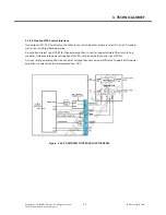
Interpolation Filter

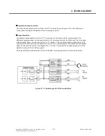
The interpolation path of the X-GOLD™110 audio front-end increases the sampling rate of the audio 

samples to the rate of the digital-to-analog converter. Because the input sampling rates can vary between 

8 kHz and 47.619 kHz the filter characteristic and oversampling ratio can be adjusted to the respective 

sampling rate. The requirements for the interpolation filters depend on the sampling rate, because a 

sufficient out-of-band discrimination in the audio frequency band (20 Hz,...,20 kHz) has to be ensured.

̲

Decimation Filter

The digital decimation filter on X-GOLD™110 has two operating modes: 8 kHz output sampling rate and 16 

kHz output sampling rate (or 16 kHz output sample rate and 16kHz bandwidth in case of doubled ASMD 

clock).

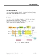
3.11.3 Analog Part

The analog part of the X-GOLD™110 audio front-end in audio-out direction consists of a stereo digital to 

analog converter (multi-bit oversampling converter) which transforms the output of the digital 

interpolation filter into analog signals. It is followed by the gain control/amplifier section. The DAC outputs 

can be switched to several output buffers. In audio-in section there is an input multiplexer which selects 

either one of two differential microphone inputs to be connected to the low-noise amplifier and analog 

pre-filter. The signals from the analog pre-filter are input to a second-order sigma-delta analog-to-digital 

converter. In addition there is a connection for FM-radio playing.

̲

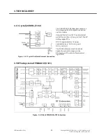
Audio-out Part

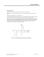
The analog audio-out part consists of two multi-bit digital-to-analogue converters (DAC) and an output 

stage. The signal sources are switched to the output drivers in the output stage. The output drivers consist 

of: a) one mono, differential class-D Loudspeaker driver, b) one mono, differential Earpiece driver and c) 

one stereo, single-ended (with uni- or bipolar signals), Headset driver.

3. TECHNICAL BRIEF

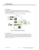
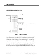
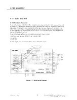
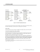
3.11.2 Digital Part

The digital part of the X-GOLDTM110 audio front-end comprises an interface to the TEAKLite® bus, 

interfaces to the interrupt units of TEAKLite®, digital interpolation filters for oversampling digital-to-analog 

conversion, digital decimation filters for analog-to-digital conversion and an interface to the analog part of 

the audio front-end.
For the digital microphone all the filtering is done in a dedicated hardware. The output sample stream is 

then fed in a duplicated ring buffer structure like the data from the analog microphone path (after A/D 

conversion and subsequent digital filtering).

Summary of Contents for GS155

Page 1: ...Service Manual Model GS155 Internal Use Only Service Manual GS155 Date February 2010 Issue 1 0 ...

Page 2: ...3 3 14Torch LED 54 3 15 Camera Interface AIT701U U405 55 4 TROUBLE SHOOTING 58 4 1 RF Component 58 4 2 RXTrouble 59 4 3TXTrouble 63 4 4 Power OnTrouble 65 4 5 ChargingTrouble 68 4 6VibratorTrouble 70 4 7 LCDTrouble 72 4 8 SpeakerTrouble 76 4 9 EarphoneTrouble 79 4 10 MicrophoneTrouble 82 4 11 SIM Card InterfaceTrouble 84 4 12 KEY backlightTrouble 86 4 13 FM RadioTrouble 88 5 DOWNLOAD 90 5 1 S W Do...

Page 3: ... LGE Internal Use Only Copyright 2010 LG Electronics Inc All right reserved Only for training and service purposes ...

Page 4: ...ommon carrier telecommunication service of facilities accessed through or connected to it The manufacturer will not be responsible for any charges that result from such unauthorized use B Incidence of Harm If a telephone company determines that the equipment provided to customer is faulty and possibly causing harm or interruption in service to the telephone network it should disconnect telephone s...

Page 5: ...look slightly different G Interference and Attenuation Phone may interfere with sensitive laboratory equipment medical equipment etc Interference from unsuppressed engines or electric motors may cause problems H Electrostatic Sensitive Devices ATTENTION Boards which contain Electrostatic Sensitive Device ESD are indicated by the sign Following information is ESD handling Service personnel should g...

Page 6: ...rop Output LDO Liquid Crystal Display LCD Intermediate Frequency IF International Portable User Identity IPUI Global System for Mobile Communications GSM General Purpose Interface Bus GPIB Gaussian Minimum Shift Keying GMSK Flexible Printed Circuit Board FPCB Electrostatic Discharge ESD Electrical Erasable Programmable Read Only Memory EEPROM Digital Signal Processing DSP dB relative to 1 milli wa...

Page 7: ...ed Oscillator VCO Universal Asynchronous Receiver Transmitter UART Time Division Multiple Access TDMA Time Division Duplex TDD Travel Adapter TA Side Tone Masking Rating STMR Pseudo SRAM PSRAM Static Random Access Memory SRAM Sending Loudness Rating SLR Subscriber Identity Module SIM Surface Acoustic Wave SAW Real Time Clock RTC Root Mean Square RMS Receiving Loudness Rating RLR Radio Frequency RF...

Page 8: ...dBm Talk time Up to 600 min GSM Tx Level 10 Charging time Approx 4 hours RX Sensitivity GSM EGSM 108dBm DCS 108dBm TX output power GSM EGSM 32 5dBm Level 5 DCS PCS 29 5dBm Level 0 SIM card type 3V Small Display MAIN 1 52 TFT 128 x 160 Status Indicator Hard icons Key Pad 0 9 Up Down Left Right Navigation Key Send Key PWR Key Soft Key Left Right ANT Internal EAR Phone Jack Yes PC Synchronization Yes...

Page 9: ... service purposes 2 PERFORMANCE ʹΠΡΪΣΚΘΙΥ ι ͽ ͶΝΖΔΥΣΠΟΚΔΤ ͺΟΔ ͲΝΝ ΣΚΘΙΥ ΣΖΤΖΣΧΖΕ ΟΝΪ ΗΠΣ ΥΣΒΚΟΚΟΘ ΒΟΕ ΤΖΣΧΚΔΖ ΡΦΣΡΠΤΖΤ ͽ Ͷ ͺΟΥΖΣΟΒΝ ΆΤΖ ΟΝΪ 9 140 2 SYSTEM SPECIFICATION Travel Adapter Yes Speaker Receiver 18x12Ȱ Speaker Receiver MIDI 32 poly Item Feature Comment Camera Yes FM Radio 87 108MHz supported ...

Page 10: ...1880 MHz 2 Phase Error RMS 5 degrees Peak 20 degrees 3 Frequency Error 0 1 ppm 4 Power Level Level Power Toler Level Power Toler 6 31dBm 3dB 14 15dBm 3dB 7 29dBm 3dB 15 13dBm 3dB 8 27dBm 3dB 16 11dBm 5dB 9 25dBm 3dB 17 9dBm 5dB 10 23dBm 3dB 18 7dBm 5dB 11 21dBm 3dB 19 5dBm 5dB 12 19dBm 3dB GSM850 EGSM 5 33dBm 2dB 13 17dBm 3dB Level Power Toler Level Power Toler 1 28dBm 3dB 9 12dBm 4dB 2 26dBm 3dB ...

Page 11: ...ue to modulation Offset from Carrier kHz Max dBc 100 0 5 200 30 250 33 400 60 600 1 200 60 1 200 1 800 60 1 800 3 000 63 3 000 6 000 65 6 000 71 GSM850 EGSM Offset from Carrier kHz Max dBc 100 0 5 200 30 250 33 400 60 600 1 200 60 1 200 1 800 60 1 800 3 000 65 3 000 6 000 65 6 000 73 DCS PCS 6 Output RF Spectrum due to switching transient GSM850 EGSM Offset from Carrier kHz Max dBm 400 19 600 21 1...

Page 12: ...ification 6 Output RF Spectrum due to switching transient Offset from Carrier kHz Max dBm 400 22 600 24 1 200 24 1 800 27 7 Spurious Emissions Conduction Emission Status 8 Bit Error Ratio GSM850 EGSM BER Class II 2 439 102 dBm DCS PCS BER Class II 2 439 100 dBm 9 RX Level Report Accuracy 3 dB 10 SLR 13 4 dB 11 Sending Response 300 12 1 000 6 2 000 6 3 000 6 Frequency Hz Max dB Min dB 100 200 4 000...

Page 13: ... 500 5 1 000 5 3 000 5 Frequency Hz Max dB Min dB 100 200 4 000 3 400 10 2 0 2 12 0 2 2 14 STMR 17 dB 㢨ㇵ Mean that Adopt a straight line in between 300 Hz and 1 000 Hz to be Max level in the range 15 Stability Margin 6 dB 16 System frequency 13 MHz tolerance 2 5 ppm 17 32 768KHz tolerance 30 ppm 18 Ringer Volume At least 65 dBspl under below conditions 1 Ringer set as ringer 2 Test distance set as...

Page 14: ...Bar Number Power 4 2 101 2 93 2 20 Antenna Display 2 1 1 0 Battery Bar Number Voltage 3 3 2 3 75 0 05 V 21 Battery Indicator 22 Low Voltage Warning Blinking Bar Once per 1 minute Receiver Once per 3 minute Speaker 23 Forced shut down Voltage 3 3 0 05V 24 Battery Type Lithium Ion Battery Standard Voltage 3 7 V Battery full charge voltage 4 2 V Capacity 950mAh 25 Travel Charger Switching mode charge...

Page 15: ...aining and service purposes 3 TECHNICAL BRIEF 3 TECHNICAL BRIEF ʹΠΡΪΣΚΘΙΥ ι ͽ ͶΝΖΔΥΣΠΟΚΔΤ ͺΟΔ ͲΝΝ ΣΚΘΙΥ ΣΖΤΖΣΧΖΕ ΟΝΪ ΗΠΣ ΥΣΒΚΟΚΟΘ ΒΟΕ ΤΖΣΧΚΔΖ ΡΦΣΡΠΤΖΤ ͽ Ͷ ͺΟΥΖΣΟΒΝ ΆΤΖ ΟΝΪ 15 140 3 TECHNICAL BRIEF 3 1 Digital Main Processor Figure 3 1 1 X Gold tm 110 Hardware Block Diagram 3 TECHNICAL BRIEF ...

Page 16: ...th a 16KB Instruction Cache and a Data cache Buffer FM Stereo Radio Receiver with RDS There are several Interfaces I2S interface for DAI connections for Tape Approval and external Audio component connection High Speed SSC Interface for connection of companion chips like Serial SD Cards High Speed SSC Interface dedicated to Display control USIM Interface with support of Protocol T 1 and Dual USIM s...

Page 17: ...piece driver 32 ȳ headset driver Measurement interfaces PA temperature battery voltage battery temperature and ambient temperature Accessory Detection PCB ID detection as part of measurement interface Differential microphone input System start up circuitry Charger circuitry for NiCd NiMh and LiIon cells with integrated Control Current Voltage Charging Integrated regulators for direct connection to...

Page 18: ...RDS Receiver Sensitivity 2 ɆV EMF Support for US EU bands Stereo recording 3 1 5 Display Type 128 128 QQVGA 65k color parallel Interface Parallel 8 9bit MIPI DBI Type B Interf voltage at 1 8V or 2 8V gRacr Display Controller Hardware 30 fps Display update without DMA up to 60 fps full or partial Video post processing Scaling Rotation 90 steps Mirroring Overlay with alpha blending Color conversion ...

Page 19: ...ctions These power supplies are generated in the integrated power management Unit PMU The PMU is designed to deliver the power for a typical standard phone Figure 3 2 1 Block Figure of the PMU Modules X Gold tm 110 3 TECHNICAL BRIEF DC DC Step Down Converter for 1 8V SD1 The DC DC converter generates a 1 8 V supply rail This voltage rail is used to supply main parts of the system like the digital ...

Page 20: ...O provides the VCORE supply used for most of the digital parts of the chip LPMU The LPMU provides VPMU sued for the PMU supply e g for the startup state machine and analog parts like ADC sense amplifier etc LAUX The LAUX generates VAUX It is a general purpose LDO and can be used for different functions depending on the phone application e g for the display or Camera LSIM The LSIM LDO generates the...

Page 21: ... Inc All right reserved Only for training and service purposes 3 TECHNICAL BRIEF ʹΠΡΪΣΚΘΙΥ ι ͽ ͶΝΖΔΥΣΠΟΚΔΤ ͺΟΔ ͲΝΝ ΣΚΘΙΥ ΣΖΤΖΣΧΖΕ ΟΝΪ ΗΠΣ ΥΣΒΚΟΚΟΘ ΒΟΕ ΤΖΣΧΚΔΖ ΡΦΣΡΠΤΖΤ ͽ Ͷ ͺΟΥΖΣΟΒΝ ΆΤΖ ΟΝΪ 21 140 3 TECHNICAL BRIEF Table 3 2 1 Power supply Domains without RF ...

Page 22: ... machine is always connected to VPMU also The power up sequence driven by the PMU state machine can be seen in Figure18 After enabling the reference HPGB and waiting for the settling time the battery voltage is measured and compared with the power on threshold If the battery voltage is high enough the SD1 DC DC converter and the LCORE LDO are started A timer ensures that the supply voltage will be...

Page 23: ...for training and service purposes 3 TECHNICAL BRIEF ʹΠΡΪΣΚΘΙΥ ι ͽ ͶΝΖΔΥΣΠΟΚΔΤ ͺΟΔ ͲΝΝ ΣΚΘΙΥ ΣΖΤΖΣΧΖΕ ΟΝΪ ΗΠΣ ΥΣΒΚΟΚΟΘ ΒΟΕ ΤΖΣΧΚΔΖ ΡΦΣΡΠΤΖΤ ͽ Ͷ ͺΟΥΖΣΟΒΝ ΆΤΖ ΟΝΪ 23 140 3 TECHNICAL BRIEF Figure 3 2 1 First Part of the State Machine Running in Different Power Domains than the Second Part ...

Page 24: ...ng and service purposes LGE Internal Use Only 3 TECHNICAL BRIEF ʹΠΡΪΣΚΘΙΥ ι ͽ ͶΝΖΔΥΣΠΟΚΔΤ ͺΟΔ ͲΝΝ ΣΚΘΙΥ ΣΖΤΖΣΧΖΕ ΟΝΪ ΗΠΣ ΥΣΒΚΟΚΟΘ ΒΟΕ ΤΖΣΧΚΔΖ ΡΦΣΡΠΤΖΤ ͽ Ͷ ͺΟΥΖΣΟΒΝ ΆΤΖ ΟΝΪ 24 140 3 TECHNICAL BRIEF Figure 3 2 2 Second Main Part of the Startup State Machine in the VPMU Domain ...

Page 25: ... read in the PMU registers so it can be used as a functional key during phone operation also 3 2 4 Switching on due to RTC alarm The real time clock can generate a wakeup signal called RTC alarm This signal is sampled from the state machine and after successfully detecting a high the system is switched on 3 2 5 Switching on due to charging When a battery with a voltage below the SSONLEV level is i...

Page 26: ... This state change is indicated to the charger state machine to enable the charger watchdog for safety 3 2 6 Power Supply Start up sequence In order to avoid an excessive drop on the battery voltage caused by in rush current during system power on possibly leading to system instability and hick ups a staggered turn on approach for the regulators is implemented The regulators are turned on in a wel...

Page 27: ...ight reserved Only for training and service purposes 3 TECHNICAL BRIEF ʹΠΡΪΣΚΘΙΥ ι ͽ ͶΝΖΔΥΣΠΟΚΔΤ ͺΟΔ ͲΝΝ ΣΚΘΙΥ ΣΖΤΖΣΧΖΕ ΟΝΪ ΗΠΣ ΥΣΒΚΟΚΟΘ ΒΟΕ ΤΖΣΧΚΔΖ ΡΦΣΡΠΤΖΤ ͽ Ͷ ͺΟΥΖΣΟΒΝ ΆΤΖ ΟΝΪ 27 140 3 TECHNICAL BRIEF Figure 3 2 3 Start Up Sequence triggered by First Connect Event ...

Page 28: ...g the vcxo_enable signal This is handled by a dedicated logic in the PMU see Figure 21 As long as rf_sysclk_en_pmu the output of the PMU state machine is high vcxo_enable controls the rf_sysclk_en signal to the RF If rf_sysclk_en_pmu is low the DXCO is switched off independent from vcxo_enable Figure 3 2 4 How sysclock Enable is Routed in the PMU 3 2 8 Undervoltage Shutdown In active mode the PMU ...

Page 29: ...ple plugging in a battery a PMU internal oscillator is used for generation of the PMU clock pmu_clock The frequency is slightly above 32 kHz typ 50 kHz to be out of the audio band also for worst case devices After first startup the software shall enable the 32 kHz crystal oscillator It is not possible to use the 32 kHz oscillator during first startup because the settling time of the oscillator can...

Page 30: ...g The DC DC converter works in different modes If the mode is switched from PFM to PWM the pulse width of the DC DC converter depends on the current battery voltage and on the output voltage The PMU state machine knows the battery voltage because of the battery supervision function Depending on this value it selects a startup pulse width for the DC DC converter out of a register table 4 values 3 2...

Page 31: ...te Transmit VCO to Antenna and Antenna to Receive SAW filter solution The FEM also supports Class 12 General Packet Radio Service GPRS multi slot operation The module consists of a GSM900 PA block and a DCS1800 PA block impedance matching circuitry for 50 ȳ input and output impedances Tx harmonics filtering high linearity and low insertion loss PHEMT RF switches diplexer and a Power Amplifier Cont...

Page 32: ...2 4 23 3 24 2 5 2 6 2 7 2 8 2 9 2 0 3 1 GND1 0 2 D N G 9 1 D N G 8 1 D N G 7 1 D N G 6 1 D N G 5 1 D N G GND2 GND14 DCS_TX ANT GND3 GND10 GSM_TX GND9 GND4 GND8 VBATT GND7 GND5 RSVD2 VLOGIC GSM_RX 4 D N G P 5 D N G P 6 D N G P P M A R V N E _ X T S B D V S R 6 D N G X R _ S C D 1 D V S R 7 D N G P 8 D N G P 9 D N G P PGND10 PGND11 PGND12 PGND13 PGND14 PGND15 6 1 D N G P 7 1 D N G P 8 1 D N G P 9 1 ...

Page 33: ...n The X GOLDTM110 RF Subsystem contains a fully integrated 26 MHz digitally controlled crystal oscillator designed for 8 pF crystals The only external part of the oscillator is the crystal itself Overall pulling range of the DCXO is approximately 55 ppm controllable by a 13 bit tuning word DCXO_AFC 16 4 The 26 MHz reference clock can also be applied to external components like Bluetooth or GPS via...

Page 34: ...0 and one high band DCS1800 or PCS1900 A block diagram of the RF subsystem is given in Figure 3 4 1 3 TECHNICAL BRIEF 3 5 2 FUNCTIONAL DESCRIPTION Figure 3 5 2 RECEIVER CHAIN BLOCK DIAGRAM 3 5 2 1 Receiver The X GOLDTM110 receiver is based on the Direct Conversion Receiver architecture DCR and can be configured to support one low band GSM850 or EGSM900 and one high band DCS1800 or PCS1900 A fully ...

Page 35: ...ctional N sigma delta synthesizer for constant envelope GMSK modulation This configuration allows a very low power design without any external components Up and down ramping is performed via the ramping DAC connected to VRAMP 3 5 2 3 RF synthesizer The X GOLDTM110 transceiver contains a fractional N sigma delta synthesizer for frequency synthesis in RX mode In TX mode the fractional N sigma delta ...

Page 36: ...5 2 4 Front end PA Control Interface Two outputs FE1 FE2 for direct control of antenna switch modules enable to select RX and TX mode as well as low and high band operation An extra band select signal PABS for the power amplifier is used to support discrete PA and switching modules Time accurate power dissipation of the PA is achieved by the control signal PAEN A minor set of power amplifiers requ...

Page 37: ... device is designed to divide its memory arrays into 135 block swith independent hardware protection This block architecture provides highly flexible erase and program capability The 64Mb NOR Flash consists of sixteen banks This device is capable of reading data from one bank while programming or erasing in the other bank Regarding read access time the device provides an 14 5ns burst access time a...

Page 38: ...on for the mobile market with its low cost high density and high performance feature device is fabricated by SAMSUNGːs advanced CMOS technology using one transistor memory cell The device supports the traditional SRAM like asynchronous operation asynchronous read and asynchronous write the NOR flash like synchronous operation synchronous burst read and asynchronous write and the fully synchronous ...

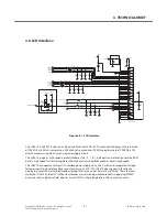
Page 39: ... to SIM card SIM_DATA This signal is interface datum The Main Base Band Processor XMM 110 provides SIM Interface Module The XMM2130 checks status Periodically During established call mode whether SIM card is inserted or not but it doesn t check during deep sleep mode In order to communicate with SIM card 3 signals SIM_DATA SIM_CLK SIM_RST And This model supports 1 8 3V SIM Card 3 TECHNICAL BRIEF J...

Page 40: ...ate voltage levels for driving an LCD The LG4515 also supports a function to display in 8 colors and a standby mode allowing for precise power control by software These features make the LG4515 an ideal LCD driver for medium or small sized portable products supporting WWW browsers such as digital cellular phones or small PDAs where long battery life is a major concern 3 TECHNICAL BRIEF 82K R401 R4...

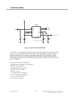
Page 41: ...ode has very low resistance allowing LED current regulation to be maintained with input supply voltage approaching the LED forward voltage The AAT3192 is available in the 2x2mm 10 lead SC70JW 10 package Drives up to 2 LEDs at up to 30mA each Automatic Switching Between 1x and 2x Modes 0 9MHz Switching Frequency Linear LED Output Current Control Single wire S2Cwire Interface AAT3192 1 16 step 10 LE...

Page 42: ...ate through constant current fast charge top off charge and full charge indication Proprietary thermal regulation circuitry limits the die temperature during fast charging or when the IC is exposed to high ambient temperatures allowing maximum charging current without damaging the IC The BQ25040 accepts input supply range from 0 3V to 28V but disables charging if the input voltages exceed 6 9V to ...

Page 43: ...261 100 R278 4 7p C285 C223 27p 27p C236 C238 27p 27p C239 C241 27p C242 27p 27p C243 KB206 KB207 KB208 KB209 KB212 KB210 KB213 KB217 KB218 KB211 KB214 KB215 KB216 KB220 VA205 KB219 VA206 VRTC 27p C260 C286 4 7p KB201 KB202 KB203 KB204 KB205 R279 100 VA207 100 R280 R281 100 VA208 VA209 100 R282 R283 100 VA210 VA211 100 R284 R285 100 VA212 VA213 100 R286 R287 100 VA214 DNI D202 KEY_IN4 KEY_IN3 KEY_...

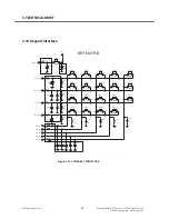
Page 44: ...ted to ground the number of keys can be extended by up to 8 keys This results in a maximum number of 72 keys to by identified by the Keypad Interface Controller The Keypad Scan Module reduces the number of interrupts and polling through the processor and therefore reduces the power consumption The module is able to debounce and scan the external keypad matrix automatically without any software int...

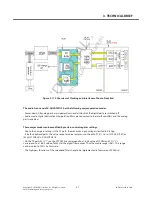
Page 45: ...one perspective called audio in and audio out subsequently It features a high quality stereo digital to analog path with amplifier stages for connecting acoustic transducers to X GOLD 110 In audio in path the supply voltage generation for electret microphones a low noise amplifier and analog to digital conversion are integrated in X GOLD 110 A more detailed functional description will be given in ...

Page 46: ... analog part is enabled These major modes can be modified by certain control register settings Due to the new gain settings in the TX path the maximum input voltage is limited to 0 8 Vpp In both voiceband paths the value range for voice samples is confined to 97 5 i e to 31948 31947 or 8334H 7CCBH in X GOLDTM110 On the TX path 83 1 s on the VTPDM line correspond to a 16 bit value of 7CCBH and 17 1...

Page 47: ...s followed by the gain control amplifier section The DAC outputs can be switched to several output buffers In audio in section there is an input multiplexer which selects either one of two differential microphone inputs to be connected to the low noise amplifier and analog pre filter The signals from the analog pre filter are input to a second order sigma delta analog to digital converter In addit...

Page 48: ...ivers can be used to drive a 16 ȳ headset They can work unipolar mode where an AC coupling of the headset might be needed or can work also in bipolor mode The differential loudspeaker driver can be used to drive a 8 ȳ loudspeaker As it is a class D amplifier the needed suppression of the higher harmonics of the switching signals has to be achieved by the external circuitry The buffers are designed...

Page 49: ...io in path consists of an input selector a low noise amplifier and following pre filter with gain control a second order ȭȟ converter and a digital decimation filter It supports both standard GSM bandwidth 3 5 kHz and wideband bandwidth 7 kHz speech bands The differential input signal from the microphone first passes a low noise amplifier and following pre filter and an anti aliasing pre filtering...

Page 50: ...F 2 microphone supplies VMIC and VUMIC are available The supply VUMIC has a ultra low power mode where the current consumption is minimum whilst at the same time the noise performance is reduced For this purpose the VUMIC is directly supplied out of the VMIC regulator the Mic Buffer can be switched off and only the quiescent current of the VMIC regulator is present This mode can be used to supply ...

Page 51: ...GHT LED Interface Key Backlight LED is controlled by switch Q202 If KEY_BCKLIGHT is high Current is flowing from VBAT to LED Then Light emitted from The LED Figure 3 12 1 Key Backlight Block 3 TECHNICAL BRIEF 1u C246 s m h o 0 6 5 R222 s m h o 0 6 5 R230 1u C258 R228 s m h o 0 6 5 R224 s m h o 0 6 5 s m h o 0 6 5 R221 10Kohms R229 s m h o 0 6 5 R227 LD201 LD202 LD203 LD204 KTC4075E_RTK H EQBN00205...

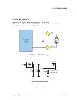
Page 52: ...ΤΖ ΟΝΪ 52 140 3 13 Vibrator Interface Support PWM signal which generated by hardware itself via register control Direct connect to the VIB and VSSVIB pin from XMM110 without any external component required It is capable to driver the vibrator motor up to 150mA Figure 3 13 1 Vibrator Driver Block Diagram 3 TECHNICAL BRIEF Figure 3 13 2 Vibrator Driver Block 47n C249 DM YK407 6F2 SJMY0007905 VB201 2...

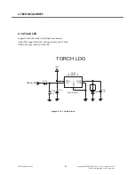
Page 53: ... ΥΣΒΚΟΚΟΘ ΒΟΕ ΤΖΣΧΚΔΖ ΡΦΣΡΠΤΖΤ ͽ Ͷ ͺΟΥΖΣΟΒΝ ΆΤΖ ΟΝΪ 53 140 3 14 Torch LED Support Torch LED which used to flash and lanterns U406 LDO support torch LED driving current up to 150mA TORCH_EN signal controls U406 LDO 3 TECHNICAL BRIEF Figure 3 14 1 Torch block 1u C412 LD401 4 3 2 1 10K R446 2 2u C438 U406 EUSY0372801 RP103K311D 5 3 2 4 1 VOUT VDD GND CE D N G P 1UF C441 VBAT TORCH_EN TORCH LDO ...

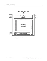
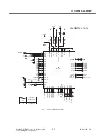
Page 54: ...ͽ Ͷ ͺΟΥΖΣΟΒΝ ΆΤΖ ΟΝΪ 54 140 3 15 Camera Interface AIT701U U405 The AIT701U is a highly integrated versatile multi media processor for image enabled mobile And handheld devices such as cellular phones and PDA AIT 701U includes and 8 bit micro controller frame display memory real time JPEGCODEC 2D Graphic Engine SD storage interface LCD Display Interface and USB interface 3 TECHNICAL BRIEF Figure 3 ...

Page 55: ...cs Inc All right reserved Only for training and service purposes 3 TECHNICAL BRIEF ʹΠΡΪΣΚΘΙΥ ι ͽ ͶΝΖΔΥΣΠΟΚΔΤ ͺΟΔ ͲΝΝ ΣΚΘΙΥ ΣΖΤΖΣΧΖΕ ΟΝΪ ΗΠΣ ΥΣΒΚΟΚΟΘ ΒΟΕ ΤΖΣΧΚΔΖ ΡΦΣΡΠΤΖΤ ͽ Ͷ ͺΟΥΖΣΟΒΝ ΆΤΖ ΟΝΪ 55 140 3 TECHNICAL BRIEF Figure 3 15 2 SENSOR SHIP BLOCK DIAGRAM ...

Page 56: ...3 PHD14 PHD15 PHLCD_BY PHLCD_A0 PHLCD_SEL PHINT PHWAIT_ PMCLK C N Y S H P C N Y S V P 0 D P 1 D P 2 D P 3 D P 4 D P PLCD2_CS_ 6 D P 7 D P N E S P A D S P K C S P K L C D P K L C _ L X P P _ T S R _ S P 0 O I P G P 1 O I P G P 2 O I P G P 3 O I P G P 4 O I P G P 5 O I P G P 6 O I P G P 7 O I P G P 0 1u C414 0 R456 0 R461 C429 33pF 3V3_VUSB 1V8_MM 1V8_MM 1u C427 100Kohms R420 C426 0 1u 0 1u C425 VAU...

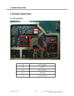
Page 57: ... SHOOTING ʹΠΡΪΣΚΘΙΥ ι ͽ ͶΝΖΔΥΣΠΟΚΔΤ ͺΟΔ ͲΝΝ ΣΚΘΙΥ ΣΖΤΖΣΧΖΕ ΟΝΪ ΗΠΣ ΥΣΒΚΟΚΟΘ ΒΟΕ ΤΖΣΧΚΔΖ ΡΦΣΡΠΤΖΤ ͽ Ͷ ͺΟΥΖΣΟΒΝ ΆΤΖ ΟΝΪ 57 140 4 1 RF Component 4 TROUBLE SHOOTING U101 Main Chip EGV3 U102 Memory U301 FEM Tx Module FL301 SAW Filter X101 Crystal 26MHz Clock 4 TROUBLE SHOOTING Figure 4 1 U301 FL301 X102 U101 U102 4 TROUBLE SHOOTING ...

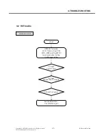
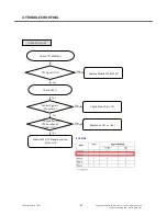
Page 58: ...ΟΔ ͲΝΝ ΣΚΘΙΥ ΣΖΤΖΣΧΖΕ ΟΝΪ ΗΠΣ ΥΣΒΚΟΚΟΘ ΒΟΕ ΤΖΣΧΚΔΖ ΡΦΣΡΠΤΖΤ ͽ Ͷ ͺΟΥΖΣΟΒΝ ΆΤΖ ΟΝΪ 58 140 START Re download SW or Do calibration again HP8960 Test mode 62 CH 7 level setting TCH 62CH 60dBm setting BCCH Spectrum analyzer setting Oscilloscope setting 1 Check Crystal Circuit 2 Check Mobile SW TX module 4 2 RX Trouble CHECKING FLOW 4 TROUBLE SHOOTING 3 Check PLL Control ...

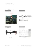
Page 59: ...ΟΥΖΣΟΒΝ ΆΤΖ ΟΝΪ 59 140 1 Checking Crystal Circuit 4 TROUBLE SHOOTING TEST POINT CIRCUIT WAVEFORM CHECKING FLOW Figure 4 2 1 26 MHz O K No Crystal is OK See next page to check PLL Circuit Yes Replace X102 Figure 4 2 2 Figure 4 2 3 X10² 1 pin 26MHz 1 pin 4 TROUBLE SHOOTING A6 A3 A4 F2 F1 A8 A9 FMRIN FMRINX XO XOX RX12 RX12X 26MHz NX3225SA X102 EXXY0018404 2 1 3 4 GND2 HOT2 HOT1 GND1 FM_ANT GSM_RXN G...

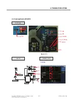
Page 60: ...3 GND10 GSM_TX GND9 GND4 GND8 VBATT GND7 GND5 RSVD2 VLOGIC GSM_RX 4 D N G P 5 D N G P 6 D N G P P M A R V N E _ X T S B D V S R 6 D N G X R _ S C D 1 D V S R 7 D N G P 8 D N G P 9 D N G P PGND10 PGND11 PGND12 PGND13 PGND14 PGND15 6 1 D N G P 7 1 D N G P 8 1 D N G P 9 1 D N G P 0 2 D N G P PGND1 PGND2 PGND3 4 7n L303 1K R302 1 2n L308 1n C309 DNI C328 SFSB0001401 FL301 B9308 10 5 3 2 6 4 7 8 9 1 I1...

Page 61: ... ΣΚΘΙΥ ΣΖΤΖΣΧΖΕ ΟΝΪ ΗΠΣ ΥΣΒΚΟΚΟΘ ΒΟΕ ΤΖΣΧΚΔΖ ΡΦΣΡΠΤΖΤ ͽ Ͷ ͺΟΥΖΣΟΒΝ ΆΤΖ ΟΝΪ 62 140 CHECKING FLOW 4 TROUBLE SHOOTING Check TP1 of SW301 TP1 Signal is OK Replace Mobile SW SW301 Yes No Yes Mobile SW TX Module and Saw Filter is OK Check Main Chip U101 Control Signal is VLogic OK No Yes Check U301 Replace FL 301 or U301 TP3 High Band TP2 Low Band Signal is OK No Yes EGSM Rx ...

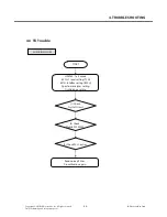
Page 62: ...62CH 60dBm setting BCCH Spectrum analyzer setting Oscilloscope setting 1 Check Crystal Circuit CHECKING FLOW 4 TROUBLE SHOOTING 2 Check Mobile SW FEM 3 Check PLL Control ʹΠΡΪΣΚΘΙΥ ι ͽ ͶΝΖΔΥΣΠΟΚΔΤ ͺΟΔ ͲΝΝ ΣΚΘΙΥ ΣΖΤΖΣΧΖΕ ΟΝΪ ΗΠΣ ΥΣΒΚΟΚΟΘ ΒΟΕ ΤΖΣΧΚΔΖ ΡΦΣΡΠΤΖΤ ͽ Ͷ ͺΟΥΖΣΟΒΝ ΆΤΖ ΟΝΪ 63 140 4 3 TX Trouble START Redownload SW or Do calibration again HP8960 Test mode 62 CH 7 level setting TCH 62CH 60dBm se...

Page 63: ...ΖΤΖΣΧΖΕ ΟΝΪ ΗΠΣ ΥΣΒΚΟΚΟΘ ΒΟΕ ΤΖΣΧΚΔΖ ΡΦΣΡΠΤΖΤ ͽ Ͷ ͺΟΥΖΣΟΒΝ ΆΤΖ ΟΝΪ 64 140 CHECKING FLOW 4 TROUBLE SHOOTING Check TP2 TP3 Mobile SW FEM is OK Yes TP5 signal same as TP1 Replace SW301 No Yes Replace PMB8810 U102 TP2 High Band TP3 Low Band Signal is OK No Yes Check PMB8810 Control Signal is VLogic TX EN BS OK No Yes Yes Check TP4 of U304 TP1 Signal is OK ReplaceFEM U304 No EGSM Tx ...

Page 64: ...ΣΚΘΙΥ ι ͽ ͶΝΖΔΥΣΠΟΚΔΤ ͺΟΔ ͲΝΝ ΣΚΘΙΥ ΣΖΤΖΣΧΖΕ ΟΝΪ ΗΠΣ ΥΣΒΚΟΚΟΘ ΒΟΕ ΤΖΣΧΚΔΖ ΡΦΣΡΠΤΖΤ ͽ Ͷ ͺΟΥΖΣΟΒΝ ΆΤΖ ΟΝΪ 64 140 4 4 Power On Trouble 4 TROUBLE SHOOTING Figure 4 4 1 Figure 4 4 3 Remote power on R116 10Kohm Figure 4 4 2 1V8_VDD VPMU VCORE VAUX VDDTRX VDDMS VDDXO VDDTDC VDD_ VRF2 VRF1 VRTC U101 100Kohms R106 10K R116 END_KEY RPWRON R116 10Kohm ...

Page 65: ... D V U M P _ T A B V U M P _ S S V 1 F R V O X D D V O X S S V C D T D D V G I D S S V F R S S V O L S S V X R T D D V O C D S S V T A B V 2 F R D D V X R T S S V S M D D V P S T A B V R S L S S V 1 P C 2 P C G E N D D V S M _ 8 V 1 _ D D V S M S S V R M F _ D D V C T R V M I S V U M P V X U A V E R O C V 1 E R O C D D V 2 E R O C D D V 1 E R O C S S V 2 E R O C S S V 3 E R O C S S V 1 U B E _ D D...

Page 66: ...el change into high of POWERKEY Check the voltage of The LDO outputs at U101 Logic level at RPWRON of R116 HIGH above 1 2V Is the phone power on The phone will Properly operating Charge or Change Battery Check the contact of power key Or dome switch Replace U101 VCORE 1 2V VPMU 1 2V VRTC 2 3V VDD_1 8V 1 8V VAUX 2 8V VDD_RF2 2 5V VRF1 1 8V VDDTRX 1 4V VDDMS 1 3V VDDXO 1 3V VDDTDC 1 3V Re download s...

Page 67: ...Ϊ ΗΠΣ ΥΣΒΚΟΚΟΘ ΒΟΕ ΤΖΣΧΚΔΖ ΡΦΣΡΠΤΖΤ ͽ Ͷ ͺΟΥΖΣΟΒΝ ΆΤΖ ΟΝΪ 67 140 4 5 Charging Trouble TEST POINT CIRCUIT Figure 4 5 1 4 TROUBLE SHOOTING Figure 4 5 2 U205 CN201 RT9524 EUSY0410801 U205 6 5 7 4 8 3 9 2 10 1 11 PGND VIN BATT ISET PGB GND1 CHGSB LDO GND2 IEOC EN_SET R231 5 1K 4 7K R265 1 2K R233 4 7K R209 C247 1UF VBAT C248 1UF VAUX VBUS_USB _CHG_EOC DSS _CHG_EN1 Single Charging IC for uUSB ...

Page 68: ...Ν ΆΤΖ ΟΝΪ 69 140 START Is I O Connector CN201 well soldered Check the voltage at Pin 1 of RT9524 5 6V Is the voltage at Pin 4 of RT9524 4 9V YES YES YES Battery is charged YES Charging is properly operating NO NO NO Resolder the CN201 Pin 1 VCHARGE The TA is out of order Change the TA Replace the U205 Replace the main board CHECKING FLOW 4 TROUBLE SHOOTING Battery is charged NO Change the battery ...

Page 69: ...69 140 4 TROUBLE SHOOTING 4 6 Vibrator Trouble TEST POINT CIRCUIT Figure 4 6 1 Figure 4 6 2 Main IC U101 Vibrator PAD u 2 2 7 2 1 C 8 0 1 C F u 1 0 2 1 F 1 1 H 1 1 F 5 1 F 4 1 F 1 1 E 9 F F E R V D N G A B I V B I V _ S S V 1 8 V 1 D D V U M P _ T A B V U M P _ S S V C131 0 22uF D D V _ 8 V 1 T A B V P _ B I V N _ B I V STAR_GND DIRTY_GND Main IC U101 47n C249 DM YK407 6F2 SJMY0007905 VB201 2 1 1U...

Page 70: ...Τ ͺΟΔ ͲΝΝ ΣΚΘΙΥ ΣΖΤΖΣΧΖΕ ΟΝΪ ΗΠΣ ΥΣΒΚΟΚΟΘ ΒΟΕ ΤΖΣΧΚΔΖ ΡΦΣΡΠΤΖΤ ͽ Ͷ ͺΟΥΖΣΟΒΝ ΆΤΖ ΟΝΪ 70 140 4 TROUBLE SHOOTING START YES NO YES Replace vibrator YES Vibrator Working well Replace the U101 NO CHECKING FLOW SETTING Enter the engineering mode and set vibrator on at vibration of BB test menu Check the Pin of vibrator Replace the Vibrator Is the voltage at VB201 high ...

Page 71: ...ning and service purposes 4 TROUBLE SHOOTING ʹΠΡΪΣΚΘΙΥ ι ͽ ͶΝΖΔΥΣΠΟΚΔΤ ͺΟΔ ͲΝΝ ΣΚΘΙΥ ΣΖΤΖΣΧΖΕ ΟΝΪ ΗΠΣ ΥΣΒΚΟΚΟΘ ΒΟΕ ΤΖΣΧΚΔΖ ΡΦΣΡΠΤΖΤ ͽ Ͷ ͺΟΥΖΣΟΒΝ ΆΤΖ ΟΝΪ 72 140 4 TROUBLE SHOOTING 4 7 LCD Trouble TEST POINT Figure 4 7 1 C406 C408 CN401 U402 R444 R441 R438 R439 R437 R435 R442 R443 R436 R434 R433 ...

Page 72: ...6 100ohms R435 100ohms R434 100ohms 100ohms R433 R432 100ohms 15pF C433 C432 15pF C431 15pF C430 15pF 1V8_VDD VAUX C421 15pF C420 15pF 1u C416 VAUX VAUX R462 100K R407 47K 1u C423 DNI R463 4 7K R404 K 7 4 5 0 4 R GF032 35S E2000 ENQY0014901 CN401 35 34 33 32 31 30 29 28 27 26 25 24 23 22 21 20 19 18 17 16 15 14 13 12 11 10 9 8 7 6 5 4 3 2 1 NLCD_RESET MLED2 MLED1 LCD_ID MLED LCD_RS L_MAIN_LCD_CS L...

Page 73: ... for training and service purposes 4 TROUBLE SHOOTING ʹΠΡΪΣΚΘΙΥ ι ͽ ͶΝΖΔΥΣΠΟΚΔΤ ͺΟΔ ͲΝΝ ΣΚΘΙΥ ΣΖΤΖΣΧΖΕ ΟΝΪ ΗΠΣ ΥΣΒΚΟΚΟΘ ΒΟΕ ΤΖΣΧΚΔΖ ΡΦΣΡΠΤΖΤ ͽ Ͷ ͺΟΥΖΣΟΒΝ ΆΤΖ ΟΝΪ 73 140 4 TROUBLE SHOOTING Waveform Graph 4 7 1 LCD Backlight Dimming Control Signal Waveform Graph 4 7 2 LCD Data Waveform ...

Page 74: ...ΟΒΝ ΆΤΖ ΟΝΪ 74 140 4 TROUBLE SHOOTING START Is the connection of CN401 with LCD connector ok NO Reassemble LCD Module and check LCD Module connection NO Check the Voltage Level of C406 and C408 is about Battery voltage W_LED_DRV signal is 1 Pulse about 75us YES Resoldering or Replace U402 NO Does LCD work properly Replace LCD module LCD working well YES CHECKING FLOW YES NO YES Check the Waveform ...

Page 75: ...for training and service purposes 4 TROUBLE SHOOTING ʹΠΡΪΣΚΘΙΥ ι ͽ ͶΝΖΔΥΣΠΟΚΔΤ ͺΟΔ ͲΝΝ ΣΚΘΙΥ ΣΖΤΖΣΧΖΕ ΟΝΪ ΗΠΣ ΥΣΒΚΟΚΟΘ ΒΟΕ ΤΖΣΧΚΔΖ ΡΦΣΡΠΤΖΤ ͽ Ͷ ͺΟΥΖΣΟΒΝ ΆΤΖ ΟΝΪ 75 140 4 8 Speaker Trouble TEST POINT Figure 4 8 1 2 TROUBLE SHOOTING Pin 3 Pin 9 C227 Pin 4 Pin 8 FB204 FB205 U204 U201 C233 ...

Page 76: ...1 A 0 1 D 0 1 B 7 A 7 B 0 1 A 9 B 2 1 C 1 1 B N S L P S L 1 N C I M 1 P C I M 2 N C I M 2 P C I M C I M U V C I M V N P E P P E L S H R S L P _ C I M N _ C I M N _ C E R P _ C E R P _ C I M _ S H N _ C I M _ S H T U O R _ P H T U O L _ P H 33n C227 330p C201 220 FB204 33n C233 30K R217 330p C202 1 0 1 4 0 0 0 Y V E S VA204 TPA6202A1ZQVR EUSY0404001 U204 B2 C1 A1 B1 B3 C2 A3 C3 IN VDD IN VO _SHUTDO...

Page 77: ... well Yes Check the Audio signal R251 R252 Yes Yes No No No Check the Audio and contorl signal U201 Pin 3 4 8 9 No Replace the U204 Yes Check the Audio signal FB204 FB205 ʹΠΡΪΣΚΘΙΥ ι ͽ ͶΝΖΔΥΣΠΟΚΔΤ ͺΟΔ ͲΝΝ ΣΚΘΙΥ ΣΖΤΖΣΧΖΕ ΟΝΪ ΗΠΣ ΥΣΒΚΟΚΟΘ ΒΟΕ ΤΖΣΧΚΔΖ ΡΦΣΡΠΤΖΤ ͽ Ͷ ͺΟΥΖΣΟΒΝ ΆΤΖ ΟΝΪ 77 140 START Cal l Check the state of contact of speaker Speaker Working well Check the Audio and control signal U201 Pin...

Page 78: ... service purposes LGE Internal Use Only 4 TROUBLE SHOOTING ʹΠΡΪΣΚΘΙΥ ι ͽ ͶΝΖΔΥΣΠΟΚΔΤ ͺΟΔ ͲΝΝ ΣΚΘΙΥ ΣΖΤΖΣΧΖΕ ΟΝΪ ΗΠΣ ΥΣΒΚΟΚΟΘ ΒΟΕ ΤΖΣΧΚΔΖ ΡΦΣΡΠΤΖΤ ͽ Ͷ ͺΟΥΖΣΟΒΝ ΆΤΖ ΟΝΪ 78 140 4 9 Earphone Trouble TEST POINT Figure 4 9 1 2 TROUBLE SHOOTING U203 C212 C256 C219 C220 FB20 1 FB20 2 CN1 ...

Page 79: ...246 C256 0 022uF R245 2 2K 4 4 2 R s m h o K 0 0 3 TP201 VBAT 0 1uF C255 C254 27pF VAUX 27pF C252 1V8_VDD R242 100Kohms 10K R241 RT8962 EUSY0406901 U203 2 B 1 C 2 C C3 A2 C4 D3 D1 D4 A1 B1 A3 B4 B3 B5 A5 C5 A4 D5 D2 BAT VB DN1 COMN1 DP2 COMP2 U1 UID U2 RES MIC AUD1 CAP AUD2 GND ISET IC L C S A D S T N I C253 FB203 120 0 1u C257 DSS FB202 600 22ohms R208 R207 22ohms C214 39pF VBUS_USB 0 022uF C212 ...

Page 80: ...er FB201 FB202 U203 C219 C220 Call or ResolderC256 C212 or Change the U203 U101 2 TROUBLE SHOOTING Check the pin 4 in CN201 is LOW U101 Change the earphone and try again ʹΠΡΪΣΚΘΙΥ ι ͽ ͶΝΖΔΥΣΠΟΚΔΤ ͺΟΔ ͲΝΝ ΣΚΘΙΥ ΣΖΤΖΣΧΖΕ ΟΝΪ ΗΠΣ ΥΣΒΚΟΚΟΘ ΒΟΕ ΤΖΣΧΚΔΖ ΡΦΣΡΠΤΖΤ ͽ Ͷ ͺΟΥΖΣΟΒΝ ΆΤΖ ΟΝΪ 80 140 START Is FB201 FB202 Signal check NO YES Resolder CN201 YES Earphone will work properly Can you hear your voice fro...

Page 81: ...ΖΣΧΚΔΖ ΡΦΣΡΠΤΖΤ ͽ Ͷ ͺΟΥΖΣΟΒΝ ΆΤΖ ΟΝΪ 81 140 4 10 Microphone Trouble TEST POINT Figure 4 10 1 2 TROUBLE SHOOTING C230 R212 C231 R213 C215 CIRCUIT 10u C231 DNI C203 C204 DNI 39pF C206 C215 0 033uF MIC201 SUMY0007102 2 1 C222 39pF C224 39pF 1 0 2 A V R210 2 2Kohms R211 1Kohms VMIC 100ohms R212 R213 100ohms R214 2 2Kohms C229 39pF 2 0 2 A V 0 033uF C230 MIC_P MIC_N 10 uF 6 3V M X5R TC 1608 R TP ECCH00...

Page 82: ...T NO YES Microphone will work properly SETTING After initialize Agilent 8960 Test EGSM900 DCS mode or GSM850 PCS mode YES Check the signal Level at each side of MIC201 Is it a few tens mV AC Check the soldering of R212 R213 C230 C215 Make a phone call then check C231 mic bias signal comes from U101 NO Change the microphone YES NO Resolder component CHECKING FLOW 1 Check mic Bias signal line 2 Chan...

Page 83: ...ΗΠΣ ΥΣΒΚΟΚΟΘ ΒΟΕ ΤΖΣΧΚΔΖ ΡΦΣΡΠΤΖΤ ͽ Ͷ ͺΟΥΖΣΟΒΝ ΆΤΖ ΟΝΪ 83 140 4 11 SIM Card Interface Trouble TEST POINT CIRCUIT Figure 4 11 1 4 TROUBLE SHOOTING PIN4 J201 PIN 6 PIN 3 PIN 1 J201 ENSY0025101 GCA26D 6S H18 E1500 9 8 10 7 6 3 5 2 4 1 C1 C5 C2 C6 C3 C7 GND1 GND4 GND2 GND3 2V85_VSIM 22pF C216 C218 68pF 2V85_VSIM 4 7Kohms R206 2V85_VSIM C225 0 1uF C250 DNI SIM_DATA SIM_CLK SIM_RST SIM_CONNECTOR ...

Page 84: ...START Does the SIM card support 3V or 1 8V NO Change the SIM Card This phone supports 3V or 1 8V SIM card YES Is Voltage at the pin1 of J201 2 85V or 1 8V NO Change the U101 NO YES Resolder J201 YES Voltage output of VSIM LDO Is 2 85V Change the SIM Card And try again Does it work Properly YES SIM card is properly working redownload SW Does it work Properly NO Change the main board NO YES SIM card...

Page 85: ...ΥΣΒΚΟΚΟΘ ΒΟΕ ΤΖΣΧΚΔΖ ΡΦΣΡΠΤΖΤ ͽ Ͷ ͺΟΥΖΣΟΒΝ ΆΤΖ ΟΝΪ 85 140 4 TROUBLE SHOOTING 4 12 KEY backlight Trouble TEST POINT Figure 4 12 1 CIRCUIT 1u C246 s m h o 0 6 5 R222 s m h o 0 6 5 R230 1u C258 R228 s m h o 0 6 5 R224 s m h o 0 6 5 s m h o 0 6 5 R221 10Kohms R229 s m h o 0 6 5 R227 LD201 LD202 LD203 LD204 KTC4075E_RTK H EQBN0020501 Q202 1 2 3 LD205 VBAT 2 2u C283 LD206 KEY_BACKLIGHT KEY BACKLIGHT ...

Page 86: ...ʹΠΡΪΣΚΘΙΥ ι ͽ ͶΝΖΔΥΣΠΟΚΔΤ ͺΟΔ ͲΝΝ ΣΚΘΙΥ ΣΖΤΖΣΧΖΕ ΟΝΪ ΗΠΣ ΥΣΒΚΟΚΟΘ ΒΟΕ ΤΖΣΧΚΔΖ ΡΦΣΡΠΤΖΤ ͽ Ͷ ͺΟΥΖΣΟΒΝ ΆΤΖ ΟΝΪ 86 140 4 TROUBLE SHOOTING START Is Pin3 of Q202 low at KEY_BACKLIGHT high NO Check Q202 Are all LEDs Working NO YES Check the soldering each R and LED Backlight will work properly NO Replace or resolder component CHECKING FLOW YES ...

Page 87: ... 88 140 4 TROUBLE SHOOTING 4 13 FM Radio Trouble TEST POINT CIRCUIT CN201 L202 C245 C244 Q305 D301 1u C321 24K R309 Q301 EQBN0019201 KTC3770V 2 1 3 22n L309 270ohms R310 R311 4 7K C324 470n 470n C326 5 1ohms R312 FM_ANT FM_ANT_1 FM_LNA_EN FM Radio LNA 56p C329 L313 220n ANT301 L301 56n FM_ANT_1 GU073 5P SD E1500 ENRY0008801 CN1 15 13 11 9 7 5 4 3 2 1 14 12 10 8 6 D201 180n L202 VBUS_USB 1n C244 6 ...

Page 88: ... NO Replace U205 A condition is good Check Bias Voltage MUIC U205 Check F Input output signal at MUIC YES NO Replace U102 A condition is good ʹΠΡΪΣΚΘΙΥ ι ͽ ͶΝΖΔΥΣΠΟΚΔΤ ͺΟΔ ͲΝΝ ΣΚΘΙΥ ΣΖΤΖΣΧΖΕ ΟΝΪ ΗΠΣ ΥΣΒΚΟΚΟΘ ΒΟΕ ΤΖΣΧΚΔΖ ΡΦΣΡΠΤΖΤ ͽ Ͷ ͺΟΥΖΣΟΒΝ ΆΤΖ ΟΝΪ 89 140 4 TROUBLE SHOOTING A condition is good START Check of ear_jack condition NO YES CHECKING FLOW FM_radio will work properly Check condition of ma...

Page 89: ... ΤΖΣΧΚΔΖ ΡΦΣΡΠΤΖΤ ͽ Ͷ ͺΟΥΖΣΟΒΝ ΆΤΖ ΟΝΪ 89 140 5 DOWNLOAD 5 1 S W Download Figure 5 1 S W download upgrade setup 5 DOWNLOAD Preparation Target terminal PIF Union RS 232 Cable and PIF UNION to Phone interface Cable Power Supply or Battery PC supporting RS 232 with Windows 2000 or newer If you are going to use battery the voltage of the battery should be over 3 7V for stable power supplying during S ...

Page 90: ...rposes LGE Internal Use Only 5 DOWNLOAD ʹΠΡΪΣΚΘΙΥ ι ͽ ͶΝΖΔΥΣΠΟΚΔΤ ͺΟΔ ͲΝΝ ΣΚΘΙΥ ΣΖΤΖΣΧΖΕ ΟΝΪ ΗΠΣ ΥΣΒΚΟΚΟΘ ΒΟΕ ΤΖΣΧΚΔΖ ΡΦΣΡΠΤΖΤ ͽ Ͷ ͺΟΥΖΣΟΒΝ ΆΤΖ ΟΝΪ 90 140 5 DOWNLOAD 5 2 Download program user guide 5 2 1 After GSMULTI folder copy paste C 5 2 2 MultiGSM exe execution file execute GS108 GS108 ...

Page 91: ...ing and service purposes 5 DOWNLOAD ʹΠΡΪΣΚΘΙΥ ι ͽ ͶΝΖΔΥΣΠΟΚΔΤ ͺΟΔ ͲΝΝ ΣΚΘΙΥ ΣΖΤΖΣΧΖΕ ΟΝΪ ΗΠΣ ΥΣΒΚΟΚΟΘ ΒΟΕ ΤΖΣΧΚΔΖ ΡΦΣΡΠΤΖΤ ͽ Ͷ ͺΟΥΖΣΟΒΝ ΆΤΖ ΟΝΪ 91 140 5 DOWNLOAD 5 3 Multi Download Program Setting Model Base Ϯ Multi Download Program Execution Setting Configuration Setting Completed GS108 GS108 ...

Page 92: ... training and service purposes LGE Internal Use Only 5 DOWNLOAD ʹΠΡΪΣΚΘΙΥ ι ͽ ͶΝΖΔΥΣΠΟΚΔΤ ͺΟΔ ͲΝΝ ΣΚΘΙΥ ΣΖΤΖΣΧΖΕ ΟΝΪ ΗΠΣ ΥΣΒΚΟΚΟΘ ΒΟΕ ΤΖΣΧΚΔΖ ΡΦΣΡΠΤΖΤ ͽ Ͷ ͺΟΥΖΣΟΒΝ ΆΤΖ ΟΝΪ 92 140 5 DOWNLOAD Stand by Condition Wait phone connecting confirm Phone connection GS108 GS108 ...

Page 93: ...ctronics Inc All right reserved Only for training and service purposes 6 BLOCK DIAGRAM ʹΠΡΪΣΚΘΙΥ ι ͽ ͶΝΖΔΥΣΠΟΚΔΤ ͺΟΔ ͲΝΝ ΣΚΘΙΥ ΣΖΤΖΣΧΖΕ ΟΝΪ ΗΠΣ ΥΣΒΚΟΚΟΘ ΒΟΕ ΤΖΣΧΚΔΖ ΡΦΣΡΠΤΖΤ ͽ Ͷ ͺΟΥΖΣΟΒΝ ΆΤΖ ΟΝΪ 93 140 6 Block Diagram 6 Block Diagram 6 BLOCK DIAGRAM ...

Page 94: ... 0 5 1 1 C F u 7 4 0 F u 1 0 6 1 1 C F u 7 4 0 0 7 1 1 C 1V8_VDD1V8_VDD Q101 1 2 3 VDDTRX VDDMS 1V8_VDD VRTC VAUX 1UF C118 F u 2 2 0 9 1 1 C R108 1 5K TP151 1V8_VDD 1V8_VDD F u 1 0 0 2 1 C F u 7 4 0 0 2 2 1 C 3 2 1 C F U 1 470ohms R109 47n C129 VDDRF2 TP150 C125 1u 22p C102 2V85_VSIM 22uF C126 1u C109 0 1u C128 10u C133 100K R111 26MHz NX3225SA X102 EXXY0018404 2 1 3 4 GND2 HOT2 HOT1 GND1 39K R112...

Page 95: ...203 C241 27p C242 27p LD202 27p C243 KB206 KB207 KB208 KB209 KB212 3V3_VUSB 10K R247 KTA2014E EQBP0006301 Q203 2 1 3 C E B KB210 LD203 10 R220 1 5K R246 C256 0 022uF KB213 KB217 KB218 KB211 KB214 1n C244 R245 2 2K 1V8_VDD KB215 4 4 2 R s m h o K 0 0 3 KB216 KB220 VA205 TP201 VBAT KB219 VA206 VRTC 0 1uF C255 R223 100K C254 27pF 200K R225 VAUX 6 8p C245 LD204 KTC4075E_RTK H EQBN0020501 Q202 1 2 3 27...

Page 96: ... A R V N E _ X T S B D V S R 6 D N G X R _ S C D 1 D V S R 7 D N G P 8 D N G P 9 D N G P PGND10 PGND11 PGND12 PGND13 PGND14 PGND15 6 1 D N G P 7 1 D N G P 8 1 D N G P 9 1 D N G P 0 2 D N G P PGND1 PGND2 PGND3 4 7n L303 1K R302 1 2n L308 1n C309 DNI C328 SFSB0001401 FL301 B9308 10 5 3 2 6 4 7 8 9 1 I1 O1_1 O1_2 O2_1 I2 O2_2 1 G 2 G 3 G 4 G L302 18n 1 2p C313 L304 1 5n 2 2nH L305 L306 2 2nH VBAT ANT...

Page 97: ...21 15pF C420 15pF 0 1uF C419 D D V D _ M A C _ 8 V 1 C418 0 1uF R419 47K 0 R418 0 1u C417 1u C416 1u C415 1V8_MM 1V8_CAM_IOVDD 2V8_CAM_AVDD VAUX 1V8_MM VAUX R462 100K 1V8_CAM_IOVDD 3 0 4 P T 0 R408 R407 47K R417 2 2K 1u C423 DNI R463 1V8_MM C413 1UF VBAT 3V3_VUSB 47K R415 47K R414 BU33TD2WNVX EUSY0407201 U401 5 3 2 4 1 VOUT VIN GND STBY D N G P 47K R413 47K R412 1V8_CAM_DVDD 47K R411 C443 1u R409 ...

Page 98: ...e purposes LGE Internal Use Only 8 BGA Pin Map 8 BGA Pin Map ʹΠΡΪΣΚΘΙΥ ι ͽ ͶΝΖΔΥΣΠΟΚΔΤ ͺΟΔ ͲΝΝ ΣΚΘΙΥ ΣΖΤΖΣΧΖΕ ΟΝΪ ΗΠΣ ΥΣΒΚΟΚΟΘ ΒΟΕ ΤΖΣΧΚΔΖ ΡΦΣΡΠΤΖΤ ͽ Ͷ ͺΟΥΖΣΟΒΝ ΆΤΖ ΟΝΪ 101 140 8 1 BGA PIN MAP Top View 8 1 1 BGA IC pin check U101 ؼ Ball Diagram Top View PMB7900 E GOLDVoice 3 Use Not Use ...

Page 99: ...All right reserved Only for training and service purposes 8 BGA Pin Map ʹΠΡΪΣΚΘΙΥ ι ͽ ͶΝΖΔΥΣΠΟΚΔΤ ͺΟΔ ͲΝΝ ΣΚΘΙΥ ΣΖΤΖΣΧΖΕ ΟΝΪ ΗΠΣ ΥΣΒΚΟΚΟΘ ΒΟΕ ΤΖΣΧΚΔΖ ΡΦΣΡΠΤΖΤ ͽ Ͷ ͺΟΥΖΣΟΒΝ ΆΤΖ ΟΝΪ 102 140 8 1 2 BGA IC pin check U102 ؼ Ball Diagram Top View K5N6433ATM Use Not Use ...

Page 100: ...nly for training and service purposes LGE Internal Use Only 8 BGA Pin Map ʹΠΡΪΣΚΘΙΥ ι ͽ ͶΝΖΔΥΣΠΟΚΔΤ ͺΟΔ ͲΝΝ ΣΚΘΙΥ ΣΖΤΖΣΧΖΕ ΟΝΪ ΗΠΣ ΥΣΒΚΟΚΟΘ ΒΟΕ ΤΖΣΧΚΔΖ ΡΦΣΡΠΤΖΤ ͽ Ͷ ͺΟΥΖΣΟΒΝ ΆΤΖ ΟΝΪ 103 140 8 1 3 BGA IC pin check U405 ؼ Ball Diagram Top View AIT701U Use Not Use ...

Page 101: ... 102 LGE Internal Use Only Copyright 2010 LG Electronics Inc All right reserved Only for training and service purposes ...

Page 102: ... 1 4 K B 2 2 0 1 T A B 7 3 1 C 2 B K 1 0 3 0 2 B K 8 0 2 B K 3 1 2 B K R221 LD201 1 3 1 C C242 C236 KB217 R280 C204 R284 R283 5 8 2 C 7 0 2 B K 9 0 2 B K 6 8 2 C 9 1 2 B K 2 0 2 B K 2 1 2 B K 5 1 2 B K KB204 VA214 VA201 C222 VA202 1 8 2 R R287 9 7 2 R 5 8 2 R 8 5 2 C 3 4 2 C VA209 4 2 2 R 2 8 2 R VA208 0 1 2 A V 4 2 2 C 1 3 2 C 1 1 2 R 6 0 2 C R212 C230 R213 R214 VA206 C215 C239 R227 C246 LD205 R2...

Page 103: ... FB101 CN402 462R 601R C101 Q205 C284 R271 C261 1PT R259 R223 522R 732C 022R 762R 862R U405 024R 611R 404PT 021C 421C 801C 521C 501C 201X 711C C118 221C 121C C223 624C U404 604R 304C 772R 164R 654R 514C 414C 524C 714C R272 R274 R273 C260 072R 402Q R101 962R 572R R449 R301 102CIM C210 C228 622C R215 VB201 C408 C406 C407 R462 534R 404R 434C C409 334R 502R 402U 112C 712R R218 R219 712C C424 L201 C202...

Page 104: ...MODE Engineering mode is designed to allow a service man engineer to view and test the basic functions provided by a handset The key sequence for switching the engineering mode on is 1809 155 Select Pressing END will switch back to non engineering mode operation Use Up and Down key to select a menu and press select key to progress the test Pressing back key will switch back to the original test me...

Page 105: ...of flash memory in GSM phone 11 AUTO CALIBRATION 11 AUTO CALIBRATION CM_GSM_MULTI Common Debug dll ocx Hot_Kimchi Model UI Multi_HK LG_UI_Ad6500_004 dll KF300d Spec_GU230_001 dwdio dll LG_RfCal_InfiKE000Ag_177 dll LG_RfTest_E5515C_122 dll xmm2130_eep008 cfg AutoSetup_GU230_001 Ezlooks Procedure_GU230_001 PwrSupply_Cmd script_001 Setup_Cal_Parameter_001 PwrSupply_Cmd DLL_PwrControlD dll Dll_SerialA...

Page 106: ...HotKimchi HK_40 exe Execute File HK_XX Æ XX is File Version ComLMPLib_1_11 dll Communication Module With PLC or Shield Box In Automation Rack Support to J S Shield Box and Tescom TC 5981A ComLMPLib_2_11 dll Communication Module With PLC or Shield Box In Automation Rack Support to J S Shield Box and Tescom TC 5981A Dll_EzLooksMQ_005 dll Communication Module with ezTray Installed In Local PC GuiTk11...

Page 107: ...ey if the Remote ON is used 1st ON state 1 Copy the file to C Cm_Gsm_Multi 2 Copy the files of Windows XXX MFCD DLL vsflex7l_ocx_regist to C Cm_Gsm_Multi dll ocx 3 Select MFCD DLL of your computer OS 4 Click on vsflex7l_ocx_regist 5 Click on Multi_HK reg 6 Connect as Fig 11 2 RS232 serial cable is connected between COM port of PC in general 7 Run HK_40exe to start calibration 8 Click Logic Operati...

Page 108: ...for training and service purposes LGE Internal Use Only 11 AUTO CALIBRATION 107 138 9 Set PORT using RS232 cable that PC can communicate with the phone 11 AUTO CALIBRATION 10 Select LOGIC MODE that you want Logic mode 1 Calibration only 2 Auto test only 3 Cal Auto ...

Page 109: ... Only Copyright 2010 LG Electronics Inc All right reserved Only for training and service purposes 11 AUTO CALIBRATION 108 138 11 AUTO CALIBRATION 11 Select the model name GS108 12 Click start button Model name Start button ...

Page 110: ...ency 124 37 975 Channel EGSM 900 32 5 dBm 32 5 dBm 32 5 dBm Max power 848 8 MHz 836 8 MHz 824 2 MHz Frequency 251 191 128 Channel GSM 850 High Middle Low Description BAND 109 138 11 AUTO CALIBRATION 11 5 AGC This procedure is for Rx calibration In this procedure We can get RSSI correction value Set band EGSM and press Start button the result window will show correction values per every power level...

Page 111: ... 112 LGE Internal Use Only Copyright 2010 LG Electronics Inc All right reserved Only for training and service purposes ...

Page 112: ...lectronics Inc All right reserved Only for training and service purposes 1 2 3 4 5 6 7 9 8 13 15 16 18 19 42 41 40 39 38 37 36 35 34 33 32 31 30 29 28 27 26 25 24 23 22 21 20 19 18 17 16 15 14 13 12 11 10 9 8 7 6 5 4 3 2 1 20 21 17 14 12 11 23 24 25 26 27 35 40 41 42 37 36 38 39 28 29 30 31 32 33 34 22 10 ...

Page 113: ... 114 LGE Internal Use Only Copyright 2010 LG Electronics Inc All right reserved Only for training and service purposes A B C D E F G H I J J I H G F E D C B A ASS Y EXPLODED VIEW ...

Page 114: ...LEX empty 0 15 WITHOUT COLOR A 1 4 MTAD00 TAPE WINDOW MTAD0119001 COMPLEX empty 0 15 WITHOUT COLOR C 3 4 MWAC00 WINDOW LCD MWAC0133601 MOLD Tempered Glass BLACK B 2 3 ACGM00 COVER ASSY REAR ACGM0159701 RED G 4 MCCZ00 CAP MCCZ0035301 COMPLEX empty BLACK 29 4 MCJN00 COVER REAR MCJN0114101 COMPLEX empty BLACK 27 4 MLAB LABEL A S MLAB0001102 C2000 USASV DIA 4 0 WHITE 38 4 MLCE00 LENS FLASH MLCE0014701...

Page 115: ...G GGZZ0005101 1 6 mm 4 5 mm MSWR3 BK N BH 2 1 6 4 5 SWCH FZB WITHOUT COLOR 35 5 ADCA00 DOME ASSY METAL ADCA0107001 WITHOUT COLOR 14 5 MCBA00 CAN SHIELD MCBA0064401 PRESS STS 0 2 WITHOUT COLOR 22 5 MIDZ00 INSULATOR MIDZ0248601 CUTTING NS WITHOUT COLOR 20 5 MIDZ01 INSULATOR MIDZ0252101 COMPLEX empty WITHOUT COLOR 5 MTAZ00 TAPE MTAZ0272601 COMPLEX empty WITHOUT COLOR 15 5 MLAZ00 LABEL MLAZ0038301 PID...

Page 116: ... 18 5 SVLM00 LCD MODULE SVLM0033401 Main 1 52 128 128 35 78 39 7 1 9 262K TFT TM LGDP4515 13 4 SAFF00 PCB ASSY MAIN SMT SAFF0270401 5 SAFC00 PCB ASSY MAIN SMT BOTTOM SAFC0143401 6 C101 CAP CHIP MAKER ECZH0001216 220 nF 10V K X5R TC 1005 R TP 6 C102 CAP CERAMIC CHIP ECCH0000115 22 pF 50V J NP0 TC 1005 R TP 6 C103 CAP CHIP MAKER ECZH0003103 0 1 uF 10V K X7R HD 1005 R TP 6 C104 CAP CERAMIC CHIP ECCH0...

Page 117: ...P 0 85t empty empty empty empty empty empty 6 C127 CAP CERAMIC CHIP ECCH0005603 2 2 uF 10V K X5R TC 1608 R TP 6 C128 CAP CHIP MAKER ECZH0003103 0 1 uF 10V K X7R HD 1005 R TP 6 C129 CAP CERAMIC CHIP ECCH0000163 47 nF 10V K X5R HD 1005 R TP 6 C132 CAP CERAMIC CHIP ECCH0000151 4 7 nF 25V K X7R HD 1005 R TP 6 C133 CAP CERAMIC CHIP ECCH0003002 10000000 pF 10V Z Y5V HD 2012 R TP empty empty empty empty ...

Page 118: ...20 39 pF 50V J NP0 TC 1005 R TP 6 C233 CAP CERAMIC CHIP ECCH0000161 33 nF 16V K X7R HD 1005 R TP 6 C234 CAP CERAMIC CHIP ECCH0005603 2 2 uF 10V K X5R TC 1608 R TP 6 C235 CAP CERAMIC CHIP ECCH0003002 10000000 pF 10V Z Y5V HD 2012 R TP empty empty empty empty empty empty 1 25 mm 6 C237 CAP CERAMIC CHIP ECCH0000117 27 pF 50V J NP0 TC 1005 R TP 6 C244 CAP CERAMIC CHIP ECCH0000143 1 nF 50V K X7R HD 100...

Page 119: ... 1005 R TP 6 C324 CAP CHIP MAKER ECZH0001217 470 nF 6 3V K X5R TC 1005 R TP 6 C326 CAP CHIP MAKER ECZH0001217 470 nF 6 3V K X5R TC 1005 R TP 6 C329 CAP CERAMIC CHIP ECCH0000117 27 pF 50V J NP0 TC 1005 R TP 6 C401 CAP CERAMIC CHIP ECCH0004904 1 uF 6 3V K X5R TC 1005 R TP 6 C403 CAP CERAMIC CHIP ECCH0004904 1 uF 6 3V K X5R TC 1005 R TP 6 C406 CAP CHIP MAKER ECZH0001215 1 uF 10V K X5R TC 1005 R TP 6 ...

Page 120: ...RAMIC CHIP ECCH0000112 15 pF 50V J NP0 TC 1005 R TP 6 C435 CAP CERAMIC CHIP ECCH0000112 15 pF 50V J NP0 TC 1005 R TP 6 C436 CAP CERAMIC CHIP ECCH0000112 15 pF 50V J NP0 TC 1005 R TP 6 C437 CAP CERAMIC CHIP ECCH0000112 15 pF 50V J NP0 TC 1005 R TP 6 C438 CAP CERAMIC CHIP ECCH0000198 2 2 uF 6 3V M X5R TC 1005 R TP 6 C439 CAP CERAMIC CHIP ECCH0000112 15 pF 50V J NP0 TC 1005 R TP 6 C440 CAP CERAMIC CH...

Page 121: ... 1005 R TP PBFREE 6 L302 INDUCTOR CHIP ELCH0001052 18 nH J 1005 R TP PBFREE 6 L303 INDUCTOR CHIP ELCH0004704 4 7 nH S 1005 R TP 6 L304 INDUCTOR CHIP ELCH0004707 1 5 nH S 1005 R TP 6 L305 INDUCTOR CHIP ELCH0004721 2 2 nH S 1005 R TP 6 L306 INDUCTOR CHIP ELCH0004721 2 2 nH S 1005 R TP 6 L308 INDUCTOR CHIP ELCH0004720 1 2 nH S 1005 R TP 6 L309 INDUCTOR CHIP ELCH0005004 22 nH J 1005 R TP 6 L313 INDUCT...

Page 122: ...P MAKER ERHZ0000443 2200 ohm 1 16W J 1005 R TP 6 R204 RES CHIP MAKER ERHZ0000405 10 Kohm 1 16W J 1005 R TP 6 R205 RES CHIP MAKER ERHZ0000406 100 Kohm 1 16W J 1005 R TP 6 R206 RES CHIP MAKER ERHZ0000485 4700 ohm 1 16W J 1005 R TP 6 R207 FILTER BEAD CHIP SFBH0008101 600 ohm 1005 6 R208 FILTER BEAD CHIP SFBH0008101 600 ohm 1005 6 R215 RES CHIP MAKER ERHZ0000488 4 7 ohm 1 16W J 1005 R TP 6 R216 RES CH...

Page 123: ...RHZ0000513 820 ohm 1 16W J 1005 R TP 6 R277 RES CHIP ERHY0000910 10 ohm 1 10W J 2012 R TP 6 R302 RES CHIP MAKER ERHZ0000404 1 Kohm 1 16W J 1005 R TP 6 R305 RES CHIP MAKER ERHZ0000201 100 ohm 1 16W F 1005 R TP 6 R307 RES CHIP MAKER ERHZ0000201 100 ohm 1 16W F 1005 R TP 6 R308 RES CHIP MAKER ERHZ0000201 100 ohm 1 16W F 1005 R TP 6 R309 RES CHIP MAKER ERHZ0000449 24 Kohm 1 16W J 1005 R TP 6 R310 RES ...

Page 124: ... 16W J 1005 R TP 6 R439 RES CHIP ERHY0003301 100 ohm 1 16W J 1005 R TP 6 R441 RES CHIP ERHY0003301 100 ohm 1 16W J 1005 R TP 6 R442 RES CHIP ERHY0003301 100 ohm 1 16W J 1005 R TP 6 R443 RES CHIP ERHY0003301 100 ohm 1 16W J 1005 R TP 6 R444 RES CHIP ERHY0003301 100 ohm 1 16W J 1005 R TP 6 R445 RES CHIP ERHY0000137 27K ohm 1 16W F 1005 R TP 6 R446 RES CHIP MAKER ERHZ0000405 10 Kohm 1 16W J 1005 R TP...

Page 125: ...Hz 20 PPM 12 5 pF 65000 ohm SMD 6 9 1 4 1 3 6 X10² X TAL EXXY0018404 26 MHz 10 PPM 8 pF 40 ohm SMD 3 2 2 5 0 6 12ppm at 30 C 85 C C0 1 0pF C1 3 6fF 26 10PPM 8 SMD R TP 5 SAFD00 PCB ASSY MAIN SMT TOP SAFD0140801 6 BAT1 MODULE ETC SMZY0018401 3 3V Cap 0 07F Size Coin 4 8 x 1 4 Pb Free Module Assembly 6 C131 CAP CHIP MAKER ECZH0001216 220 nF 10V K X5R TC 1005 R TP 6 C206 CAP CERAMIC CHIP ECCH0000120 ...

Page 126: ...65 475nm 95mW empty empty 2P 6 LD205 DIODE LED CHIP EDLH0015101 BLUE 1608 R TP Topview LED BLUE 2 7 3 2V 25mA 18 45mcd 465 475nm 95mW empty empty 2P 6 LD206 DIODE LED CHIP EDLH0015101 BLUE 1608 R TP Topview LED BLUE 2 7 3 2V 25mA 18 45mcd 465 475nm 95mW empty empty 2P 6 R210 RES CHIP MAKER ERHZ0000443 2200 ohm 1 16W J 1005 R TP 6 R211 RES CHIP MAKER ERHZ0000404 1 Kohm 1 16W J 1005 R TP 6 R212 RES ...

Page 127: ...UILD UP 4 GS150 V41 6 VA201 VARISTOR SEVY0003901 5 5 V SMD Vdc 5 5 Vb 8 Cp 420 1 0 0 5 0 6 5 5 480 1 0 0 5 0 6 empty SMD R TP 6 VA202 VARISTOR SEVY0003901 5 5 V SMD Vdc 5 5 Vb 8 Cp 420 1 0 0 5 0 6 5 5 480 1 0 0 5 0 6 empty SMD R TP 6 VA205 VARISTOR SEVY0004101 5 6 V SMD 360pF 1005 6 VA206 VARISTOR SEVY0004101 5 6 V SMD 360pF 1005 6 VA207 VARISTOR SEVY0004101 5 6 V SMD 360pF 1005 6 VA208 VARISTOR S...

Page 128: ... LGE Internal Use Only 12 EXPLODED VIEW REPLACEMENT PART LIST by SBOM standard on GCSC Level Location No Description Part Number Spec Color Remark 4 SUSY00 SPEAKER SUSY0028904 PIN 8 ohm 91 dB 1812 mm 3 0t contact empty 9 12 3 Accessory Note This Chapter is used for reference Part order is ordered ...

Reviews: