background image

4-4

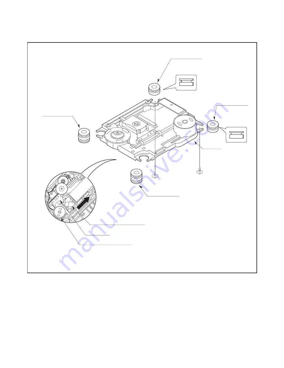
3. Base Assembly Sled (Fig. 4-3)

1) Release 4 Screw(S2).
2) Disconnect the FFC Connector(C1)

3-1. Gear Feed
3-2. Gear Middle

3-3. Gear Rack

1) Release the Scerw(S3)

4. Rubber Rear (Fig. 4-3) 

BASE PU

RUBBER DAMPER

RUBBER DAMPER

RUBBER DAMPER

Distinguish upper and 
lower sides
(Assemble with care)

Distinguish upper and 
lower sides
(Assemble with care)

RUBBER DAMPER

GEAR RACK

GENERAL PICK UP ASSEMBLY

SPINDLE MOTOR ASSEMBLY

Fig. 4-3

(S2)

(S2)

Copyright © 2009 LG Electronics. Inc. All right reserved.

Only for training and service purposes

LGE Internal Use Only

Summary of Contents for HT303SU

Page 1: ...MODEL HT303PD HT303PD D0 SH33PD F S W SERVICE MANUAL DVD CD RECEIVER SERVICE MANUAL MODEL HT303PD HT303PD D0 SH33PD F S W Website http biz lgservice com Internal Use Only P NO AFN73178958 JUNE 2009 ...

Page 2: ... 2 13 INTERNAL BLOCK DIAGRAM OF ICs 2 25 WIRING DIAGRAM 2 45 OVERALL BLOCK DIAGRAM 2 47 CIRCUIT DIAGRAMS 2 49 PRINTED CIRCUIT DIARGAMS 2 69 SECTION 3 EXPLODED VIEWS 3 1 CABINET AND MAIN FRAME SECTION 3 1 DECK MECHANISM EXPLODED VIEW DP 12TV 3 3 PACKING ACCESSORY SECTION 3 5 SPEAKER SECTION 3 6 SECTION 4 MECHANISM DP 12TV 4 1 SECTION 5 REPLACEMENT PARTS LIST 5 1 Copyright 2009 LG Electronics Inc Al...

Page 3: ...beams to enter the eyes Also NEVER switch ON the power to the laser output part lens etc of the pick up if it is damaged 5 Cleaning the lens surface If there is dust on the lens surface the dust should be cleaned away by using an air bush such as used for camera lens The lens is held by a delicate spring When cleaning the lens surface therefore a cotton swab should be used taking care not to disto...

Page 4: ...pply lead wire from the unit 2 All equipment measuring instruments and tools must be grounded 3 The workbench should be covered with a conductive sheet and grounded When removing the laser pick up from its conductive bag do not place the pick up on the bag This is because there is the possibility of damage by static electricity 4 To prevent AC leakage the metal part of the soldering iron should be...

Page 5: ... propelled chemicals These can generate electrical charges sufficient to damage ESD devices 6 Do not remove a replacement ESD device from its protective package until immediately before you are ready to install it Most replacement ESD devices are packaged with leads electrically shorted together by conductive foam aluminum foil or comparable conductive materials 7 Immediately before removing the p...

Page 6: ...e control Pause key 1 4 7 2 in order Press number 0 9 Press character A F 1 6 for a while Use arrow key to move to appropriate position and make changes Press pause key once Change will be applied when power OFF ON DETECT NEW EEPROM OPTION EDIT SCREEN HEX 53 45 20 FD 22 05 EC 32 AC 00 00 00 00 00 00 00 NAME OPT 1 OPT 2 OPT 3 OPT 4 OPT 5 OPT 6 OPT 7 OPT 8 OPT 9 OPT A OPT B OPT C OPT D OPT E OPT F O...

Page 7: ...iate position and make changes Press ENTER key once FLD write ok or up ok Remote control 2 Front STOP push same timing FLD display E2P CLR or EP CLR Auto power off NAME HEX OPT 1 82 OPT 2 CA OPT 3 22 OPT 4 27 OPT 5 00 DETECT NEW EEPROM OPTION EDIT SCREEN Copyright 2009 LG Electronics Inc All right reserved Only for training and service purposes LGE Internal Use Only ...

Page 8: ...lete message 2 How to update DVD program Update using CD 1 Rename the filename to download as TARGET BIN in upper cases 2 Copy the file to MTK_UPG folder of CD and burn it ex P MTK_UPG TARGET BIN 3 Insert the CD to the SET then after a while the CD tray will be opened with upgrade information on the screen 4 Remove the CD and press UP key in remote controller 5 Remove and reconnect the power cable...

Page 9: ...ut Power 30 W 4 Ωat 1 kHz THD 10 Subwoofer 75 W Rated Output Power 60 W 8 Ωat 30 Hz THD 10 SPEAKERS Front Speaker Center Rear Speaker Passive Subwoofer SH33PD F SH33PD S SH33PD W Impedance 4 Ω 4 Ω 8 Ω Net Dimensions 260 x 1100 x 260 mm 99 x 114 x 86 mm 156 x 325 x 320 mm W x H x D Net Weight 1EA 3 0 kg 0 37 kg 3 5 kg Designs and specifications are subject to change without notice Depending on the ...

Page 10: ...r circuit Check focus circuit Check disc NO Check tracking servo circuit NO Check audio circuit Does red power led turn on YES Is power on YES Does red power led turn on YES Does it play YES Does it output audio YES YES Turn power on INSERT POWER CORD OK Copyright 2009 LG Electronics Inc All right reserved Only for training and service purposes LGE Internal Use Only ...

Page 11: ...S Check if the front power is ok Is the Digitron on correctly NO NO Check pattern and resoldering YES Check if RC2 is ok Check if the remote control is ok YES Check if all buttons are ok POWER ON Front B D ok 1 2 Copyright 2009 LG Electronics Inc All right reserved Only for training and service purposes LGE Internal Use Only ...

Page 12: ... circuit 2 NO Refer to power SMPS NO Check RM circuit Check if the power part of the front is ok YES NO Refer to MICOM circuit Check if the remote control waveform of PN301 pin5 is ok YES Check if RC2 voltage is ok 5V YES Resolder or Replace RC2 Copyright 2009 LG Electronics Inc All right reserved Only for training and service purposes LGE Internal Use Only ...

Page 13: ...OPEN CLOSE Key Receive CLOSE Key SLED moves to inner position 1 Judge whether have disc and disc type 2 Jump to related disc reading procedure 1 Execute Pressed Key IR Key 2 System operation routine loop NO NO NO NO YES 1 Stop Playback OpenTray 2 Display tray open message LOGO POWER ON Copyright 2009 LG Electronics Inc All right reserved Only for training and service purposes LGE Internal Use Only...

Page 14: ...tem reset circuit 3 Check FLASH R W enable signal PRD RWR 4 Check FLASH Memory related circuit NO Replace FLASH Are the DCVoltage outputs OK 12V 5 6V 3 5V 5V 7V 34V YES Are 3 5V and 5V DC outputs normal on main PCBA YES YES Update FLASH successfully YES Switch on the Power PCBA TEST A Copyright 2009 LG Electronics Inc All right reserved Only for training and service purposes LGE Internal Use Only ...

Page 15: ...L IC501 Pins99 102 103 104 MT1389 L VIDEO outputs properly Show LOGO NO NO Check the load OPEN CLOSE switch Check AV cable connection between main PCBA and loader MECHA YES YES YES Normal OPEN_SW CLOSE_SW signal NO Check the Tray control IO pins on MT1389 L Normal TROPEN TRCLOSE signal NO Check the Tray control MOTOR SERVO circuit IC401 Normal LOAD LOAD signal Does Tray move inside when it is not ...

Page 16: ...on motor driver SLED and SLED output properly Does the SLED move to inner side when it is at outer position NO NO Check Focus connection on MT1389 L and motor driver Check cable connection with pick up head YES YES Proper Focus outputs to motor dricer NO Check the amp circuit on motor driver Proper F F outputs Optical Lens has movements for searching Focus B C Copyright 2009 LG Electronics Inc All...

Page 17: ...ltage of power transistor is OK Q401 Q402 Laser turns on when reading disc Put disc in NO NO Check the SPINDLE related circuit on MT1389 L Check the cable connection between spindle and main PCB YES YES Proper SPINDLE signal on MT1389 L NO Check the spindle control amp circuit of motor driver SPNP SPNN output properly Does spindle rotate NO NO Check the related circuit on MT1389 L RF signal Proper...

Page 18: ...oper CD DVDCT signal on MT1389 L Focus on ok NO Check RF signal waveform Disc Playback NO NO Check the related circuit on MT1389 L NO Check the TRACK connection on MT1389 L and motor driver NO Check the tracking control amp circuit on motor driver Proper CD DVDCT signal on MT1389 L YES Proper TRACK signal on MT1389 L YES TR TR output properly Track On OK D E Copyright 2009 LG Electronics Inc All r...

Page 19: ...S YES PWM IC received correct data stream NO Check the related circuit of PWM Check Audio out Pins 55 59 61 62 68 71 75 Normal PWM IC out IC704 Normal Audio output when disc playback E TEST END Copyright 2009 LG Electronics Inc All right reserved Only for training and service purposes LGE Internal Use Only ...

Page 20: ...54 LOW signal 0V YES NO Replace the Q701 and Q702 Is the Q701 and Q702 normal YES YES After unplug power cord connect again YES Power on PROTECTION appears on the FLD Replace ST AMP IC IC702 and IC703 Copyright 2009 LG Electronics Inc All right reserved Only for training and service purposes LGE Internal Use Only ...

Page 21: ...m insert is OK Check Power YES YES YES Replace IC101 YES NO NO NO NO Refer to SMPS NO Refer to oscillator circuit NO Check IC101 reset waveform NO NO YES Check power part of Main B D Check oscillator of X101 Check if IC101 Pin5 is high YES YES YES Check 3 3V line NO Check power section circuit NO Check if IC101 Pin9 36 59 are high 5V Check if IC101 Pin49 is high YES YES Copyright 2009 LG Electroni...

Page 22: ...LOCK RESET FLASH R W SIGNAL 1 MT1389 L main clock is at 27MHz X501 1 3 2 4 FIG 1 1 2 MT1389 L reset is high active Power Cord in FIG 1 2 1 1 2 3 4 1 2 3 4 IC501 Copyright 2009 LG Electronics Inc All right reserved Only for training and service purposes LGE Internal Use Only ...

Page 23: ...is at 27MHz X501 DCLK 93MHz Vp p 2 2 Vmax 2 7V FIG 2 1 3 Flash R W enable signal during download Downloading FIG 1 4 1 2 1 1 2 1 Copyright 2009 LG Electronics Inc All right reserved Only for training and service purposes LGE Internal Use Only ...

Page 24: ...3 TRAY OPEN CLOSE SIGNAL 1 Tray open close waveform FIG 3 1 2 Tray close waveform FIG 3 2 2 1 3 4 1 2 3 4 1 2 3 4 1 2 3 4 Copyright 2009 LG Electronics Inc All right reserved Only for training and service purposes LGE Internal Use Only ...

Page 25: ...2 16 4 SLED CONTROL RELATED SIGNAL NO DISC CONDITION FIG 4 1 1 2 3 4 1 2 3 4 Copyright 2009 LG Electronics Inc All right reserved Only for training and service purposes LGE Internal Use Only ...

Page 26: ...ATED SIGNAL NO DISC CONDITION FIG 6 1 5 LENS CONTROL RELATED SIGNAL NO DISC CONDITION FIG 5 1 1 3 2 1 3 2 1 2 3 1 2 3 Copyright 2009 LG Electronics Inc All right reserved Only for training and service purposes LGE Internal Use Only ...

Page 27: ... 18 FIG 7 2 DVD 7 DISC TYPE JUDGEMENT WAVEFORMS FIG 7 1 DVD 1 2 3 IC501 IC501 1 2 3 1 2 3 Copyright 2009 LG Electronics Inc All right reserved Only for training and service purposes LGE Internal Use Only ...

Page 28: ...2 19 FIG 7 4 CD FIG 7 3 CD 1 2 3 IC501 IC501 1 2 3 1 2 3 Copyright 2009 LG Electronics Inc All right reserved Only for training and service purposes LGE Internal Use Only ...

Page 29: ...2 20 FIG 8 2 CD 8 FOCUS ON WAVEFORMS FIG 8 1 DVD 1 2 3 1 2 3 4 4 1 2 4 3 IC501 Copyright 2009 LG Electronics Inc All right reserved Only for training and service purposes LGE Internal Use Only ...

Page 30: ...S NO DISC CONDITION FIG 9 1 10 TRACKING CONTROL RELATED SIGNAL System checking FIG 10 1 DVD 1 2 3 1 1 2 3 1 2 3 4 IC501 Copyright 2009 LG Electronics Inc All right reserved Only for training and service purposes LGE Internal Use Only ...

Page 31: ...389 L VIDEO OUTPUT WAVEFORMS 1 Full colorbar signal COMPOSIT FIG 11 1 FIG 10 2 CD 3 4 2 1 1 2 4 1 3 Copyright 2009 LG Electronics Inc All right reserved Only for training and service purposes LGE Internal Use Only ...

Page 32: ... Audio related Signal FIG 12 1 2 Y FIG 11 2 12 AUDIO OUTPUT FROM mt1389 L 1 1 3 2 IC501 IC501 1 1 2 3 Copyright 2009 LG Electronics Inc All right reserved Only for training and service purposes LGE Internal Use Only ...

Page 33: ...720 TP711 3 R704 TP707 or R717 TP705 4 R709 TP713 5 R707 TP702 6 R701 TP708 13 DVD AMP WAVEFORMS 6 5 1 4 3 2 Copyright 2009 LG Electronics Inc All right reserved Only for training and service purposes LGE Internal Use Only ...

Page 34: ...12 85 RA2 V14 13 84 DVDD33 REXT 14 83 RA1 MDI1 15 82 RA0 MDI2 16 81 RA10 LDO1 17 80 BA1 LDO2 18 79 DVSS18 AVDD33_2 19 78 BA0 DMO 20 77 RAS FMO 21 76 CAS TRAY_OPEN 22 75 RWE TRAY_CLOSE 23 74 RA4 TRO 24 73 RA5 FOO 25 72 RA6 26 71 RA7 USB_DP 27 70 RA8 USB_DM 28 69 RA9 VDD33_USB 29 68 DVDD33 VSS33_USB 30 67 RA11 PAD_VRT 31 66 RCLK VDD18_USB 32 65 DQM1 33 34 35 36 37 38 39 40 41 42 43 44 45 46 47 48 49...

Page 35: ...bug Port SDPIF Audio DAC System CP U IR VFD De interlacer CPPM CPR M DRM 32 bit RISC Motor Drive PCM output Internal 6ch Audio DACs 6ch Audio Analog outputs Audio Mic1 Audio Mic2 Internal Audio ADC USB 2 0 High Speed controller MS SD MMC Card Controller USB 2 0 High Full Speed Device MS SD MMC Flash Card 1 IC501 MPEG MT1389L BLOCK DIAGRAM Copyright 2009 LG Electronics Inc All right reserved Only f...

Page 36: ...O1 Analog Output Laser driver output 18 LDO2 Analog Output Laser driver output 19 AVDD33_2 Analog Power Analog 3 3V power 20 DMO Analog Output Disk motor control output PWM output 21 FMO Analog Output Feed motor control PWM output 22 TRAY_OPEN Analog Output Tray PWM output Tray open output 23 TRAY_CLOSE Analog Output Tray PWM output Tray close output 24 TRO Analog Output Tracking servo output PDM ...

Page 37: ...woofer channel output 2 While internal audio DAC not used a ACLK b GPIO 115 ARS GPIO Analog Output 1 Audio DAC right Surround channel output 2 While internal audio DAC not used a ABCK b GPIO 1 Audio DAC right channel output 2 While internal audio DAC not used 116 AR Analog Output a SDATA2 b GPIO c RXD2 117 AV CM Analog Audio DAC reference voltage 118 AL GPIO Analog Output 1 Audio DAC left channel ...

Page 38: ...erial Flash Clock PD SMT 40 UP1_6 SCL InOut 1 Microcontroller port 1 6 8mA SR 2 I2C clock pin PU SMT 41 UP1_7 SDA InOut 1 Microcontroller port 1 7 4mA SR 2 I2C data pin PU SMT 42 ICE Input Microcontroller ICE mode enable PD SMT 43 PRST Input Power on reset input active low PU SMT 44 IR Input IR control signal input SMT Dram Interface 37 Sorted by position 45 RD0 InOut DRAM data 0 4mA 46 RD1 InOut ...

Page 39: ...put DRAM Write enable active low 4mA PD 76 CAS Output DRAM column address strobe active low 4mA PD 77 RAS Output DRAM row address strobe active low 4mA PD 78 BA0 InOut DRAM bank address 0 4mA PD 80 BA1 InOut DRAM bank address 1 4mA PD 81 RA10 InOut DRAM address 10 4mA PD 82 RA0 InOut DRAM address 0 4mA PD 83 RA1 InOut DRAM address 1 4mA PD 85 RA2 InOut DRAM address 2 4mA PD 86 RA3 InOut DRAM addre...

Page 40: ...10 InOut 4 ASDATA0 4mA PD 5 ALRCK 6 HSYN VSYN output 7 C3 8 TXD1 1 GPIO11 2 SD_CMD set B 92 GPIO11 InOut 3 MS_BS set B 4mA PD 4 Audio Mute 5 HSYN VSYN output 6 C4 93 SPDIF GPIO12 InOut 1 SPDIF output 2mA PD 2 GPIO12 1 GPIO13 94 GPIO13 InOut 2 SD_D0 set B 4mA PD 3 ALRCK 4 Audio Mute 5 YUVCLK Copyright 2009 LG Electronics Inc All right reserved Only for training and service purposes LGE Internal Use...

Page 41: ...2 32 2 IC401 MOTOR DRIVER PIN CONFIGURATION BLOCK DIAGRAM Copyright 2009 LG Electronics Inc All right reserved Only for training and service purposes LGE Internal Use Only ...

Page 42: ...2 33 1 IC501 MPEG MT1389L PIN DESCRIPTION Copyright 2009 LG Electronics Inc All right reserved Only for training and service purposes LGE Internal Use Only ...

Page 43: ...8 P71 INT1 T0HCP AN9 P72 INT2 T0IN NKIN P73 INT3 T0IN RES XT1 AN10 XT2 AN11 VSS1 CF1 CF2 VDD1 P80 AN0 P81 AN1 P82 AN2 P10 SO0 P11 SI0 SB0 P32 UTX1 P33 URX1 P34 UTX2 P35 URX2 P36 P37 P27 INT5 T1IN P26 INT5 T1IN P25 INT5 T1IN P24 INT5 T1IN INT7 P23INT4 T1IN P22 INT4 T1IN P21 INT4 T1IN P20 INT4 T1IN INT6 P07 T7O P06 T6O P12 SCK0 P13 SO1 P14 SI1 SB1 P15 SCK1 P16 T1PWML P17 T1PWMH BUZ PWM2 PWM3 V DD 2 ...

Page 44: ...8 ADC ALU Flash ROM PC ACC B register C register PSW RAR RAM Stack pointer Watchdog timer CF RC X tal MRC Clock generator UART2 On chip Debugger ROM correct PWM2 3 UART1 Base timer Port C Timer 6 INT0 to INT7 Noise filter Port 3 Timer 7 Copyright 2009 LG Electronics Inc All right reserved Only for training and service purposes LGE Internal Use Only ...

Page 45: ...rt 2 8 bit I O port I O specifiable in 1 bit units Pull up resistor can be turned on and off in 1 bit units Other functions P20 INT4 input HOLD reset input timer 1 event input timer 0L capture input timer 0H capture input INT6 input timer 0L capture 1 input P21 to P23 INT4 input HOLD reset input timer 1 event input timer 0L capture input timer 0H capture input P24 INT5 input HOLD reset input timer...

Page 46: ...ter input port AN0 P80 to AN6 P86 No PWM2 PWM3 I O PWM2 and PWM3 output ports General purpose I O available No Port 3 P30 to P37 I O 8 bit I O port I O specifiable in 1 bit units Pull up resistor can be turned on and off in 1 bit units Pin functions P32 UART1 transmit P33 UART1 receive P34 UART2 transmit P35 UART2 receive Yes Port C PC0 to PC7 I O 8 bit I O port I O specifiable in 1 bit units Pull...

Page 47: ...CDOUT AGND OVFL SCL CCLK AD0 CS AD1 CDIN VLC RESET AIN3A AIN3B AIN2A AIN2B AIN1A AIN1B VA AFILTB VQ TSTO FILT TSTO AIN4A MICIN1 AIN4B MICIN2 AIN5A AIN5B AFILTA TSTO NC NC AGND AGND VA PGAOUTB PGAOUTA AIN6B AIN6A MICBIAS INT VD DGND MCLK LRCK SCLK SDOUT NC NC NC TSTI CS5345 Copyright 2009 LG Electronics Inc All right reserved Only for training and service purposes LGE Internal Use Only ...

Page 48: ... Right Analog Input 2 AIN3A Left Analog Input 3 10 µF 10 µF 1800 pF 1800 pF 100 k 100 k 100 100 AIN3B Right Analog Input 3 AIN4A MICIN1 Left Analog Input 4 10 µF 10 µF 1800 pF 1800 pF 100 k 100 k 100 100 AIN4B MICIN2 Right Analog Input 4 AIN5A Left Analog Input 5 10 µF 10 µF 1800 pF 1800 pF 100 k 100 k 100 100 AIN5B Right Analog Input 5 AINA Left Analog Input 10 µF 10 µF 1800 pF 1800 pF 100 k 100 ...

Page 49: ...udio inter face Refer to the Recommended Operating Conditions for appropriate voltages TSTI 37 Test Pin Input This pin must be connected to ground NC 38 39 40 No Connect These pins are not connected internally and should be tied to ground to minimize any potential coupling effects SDOUT 41 Serial AudioData Output Output Output for two s complement serial audio data SCLK 42 Serial Clock Input Outpu...

Page 50: ...IC_LRCK MIC_BCK MIC_MCLK PWM_HP_R_P IO_VSS PWM2_P PWM2_M PWM3_P PWM3_M PWM4_P PWM4_M SPI I2C CS I2C_AD2 SI I2C_AD0 SO SDA SCK SCL RESET SCAN_ENA XIN DVSS IO_VSS IO_VSS IO_VSS DVDD DVSS IO_VDD IO_VSS MSDIN1 MSDIN2 SLRCK SBCK DVSS PWM5_P PWM5_M DVDD TEST_MODE3 DVSS IO_VSS PWM6_P PWM6_M IO_VSS IO_VSS PWM1_P PWM1_M OVERLOAD IO_VSS IO_VSS SSDIN1 EXT_MUTE DVDD IO_VDD DVDD SSDIN0 MSDIN3 SSDIN2 SSDIN3 IO_...

Page 51: ...r output pin PCM Audio Input Output Interface MBCK 11 I O PCM bit clock input output of main 8 channel audio User can select the master slave mode of this signal Schmitt Trigger input MLRCK 12 I O PCM Word clock left right clock input output of main 8 channel audio User can select the master slave mode of this signal Schmitt Trigger input MSDIN 3 0 15 16 17 18 I PCM serial data input of main 8 cha...

Page 52: ...tput of channel 3 PWM3_M 54 O Negative PWM output of channel 3 PWM4_P 59 O Positive PWM output of channel 4 PWM4_M 58 O Negative PWM output of channel 4 PWM5_P 62 O Positive PWM output of channel 5 PWM5_M 61 O Negative PWM output of channel 5 PWM6_P 68 O Positive PWM output of channel 6 PWM6_M 67 O Negative PWM output of channel 6 PWM7_P 71 O Positive PWM output of channel 7 PWM7_M 70 O Negative P...

Page 53: ...er power device enable output Active High Test Mode TEST_MODE1 97 I Test mode selection pin 1 In normal operation it should be LOW or not connected Internal pull down resistor TEST_MODE2 98 I Test mode selection pin 2 In normal operation it should be LOW or not connected Internal pull down resistor SCAN_ENA 99 I Scan enable Active High In normal operation it should be LOW or not connected Internal...

Page 54: ...6 WIRING DIAGRAM PN202 CABLE1 18PIN WIRING DIAGRAM HT303 HT353 EBY38558901 8 REV 8 2 2008 12 16 Copyright 2009 LG Electronics Inc All right reserved Only for training and service purposes LGE Internal Use Only ...

Page 55: ...48 OVERALL BLOCK DIAGRAM MT1389FE L BLOCK DIAGRAM HT303 HT353 EBY38558901 7 REV 8 2 2008 12 16 Copyright 2009 LG Electronics Inc All right reserved Only for training and service purposes LGE Internal Use Only ...

Page 56: ...THE LG CORPORATION ALL COMPONENTS SHOULD BE REPLACED ONLY WITH TYPES IDENTI CAL TO THOSE IN THE ORIGINAL CIRCUIT SPECIAL COMPONENTS ARE SHADED ON THE SCHEMATIC FOR EASY IDENTIFICATION THIS CIRCUIT DIAGRAM MAY OCCASIONALLY DIF FER FROM THE ACTUAL CIRCUIT USED THIS WAY IMPLEMENTATION OF THE LATEST SAFETY AND PERFORMANCE IMPROVEMENT CHANGES INTO THE SET IS NOT DELAYED UNTIL THE NEW SERVICE LITERATURE...

Page 57: ...MPEG PART HT303 HT353 EBY38558901 1 REV 8 2 2008 12 16 A 1 2 3 4 5 6 7 8 9 10 11 12 B C D E F G H I J K L M N O P Q R S T Copyright 2009 LG Electronics Inc All right reserved Only for training and service purposes LGE Internal Use Only ...

Page 58: ...M SERVO HT303 HT353 EBY38558901 2 REV 8 2 2008 12 16 A 1 2 3 4 5 6 7 8 9 10 11 12 B C D E F G H I J K L M N O P Q R S T Copyright 2009 LG Electronics Inc All right reserved Only for training and service purposes LGE Internal Use Only ...

Page 59: ...M MICOM HT303 HT353 EBY38558901 3 REV 8 2 2008 12 16 A 1 2 3 4 5 6 7 8 9 10 11 12 B C D E F G H I J K L M N O P Q R S T Copyright 2009 LG Electronics Inc All right reserved Only for training and service purposes LGE Internal Use Only ...

Page 60: ...M I O HT303 HT353 EBY38558901 4 REV 8 2 2008 12 16 A 1 2 3 4 5 6 7 8 9 10 11 12 B C D E F G H I J K L M N O P Q R S T Copyright 2009 LG Electronics Inc All right reserved Only for training and service purposes LGE Internal Use Only ...

Page 61: ...M AMP HT303 HT353 EBY38558901 5 REV 8 2 2008 12 16 A 1 2 3 4 5 6 7 8 9 10 11 12 B C D E F G H I J K L M N O P Q R S T Copyright 2009 LG Electronics Inc All right reserved Only for training and service purposes LGE Internal Use Only ...

Page 62: ...AM MIC HT303 HT353 EBY38558901 6 REV8 2 2008 12 16 A 1 2 3 4 5 6 7 8 9 10 11 12 B C D E F G H I J K L M N O P Q R S T Copyright 2009 LG Electronics Inc All right reserved Only for training and service purposes LGE Internal Use Only ...

Page 63: ...IAGRAM A 1 2 3 4 5 6 7 8 9 10 11 12 B C D E F G H I J K L M N O P Q R S T FRONT HT303 EBY39798401 REV5 1 2007 11 30 Copyright 2009 LG Electronics Inc All right reserved Only for training and service purposes LGE Internal Use Only ...

Page 64: ...AGRAM A 1 2 3 4 5 6 7 8 9 10 11 12 B C D E F G H I J K L M N O P Q R S T PWR KEY HT303 EBY39799101 1 REV2 1 2007 11 30 Copyright 2009 LG Electronics Inc All right reserved Only for training and service purposes LGE Internal Use Only ...
Page 65: ...IAGRAM A 1 2 3 4 5 6 7 8 9 10 11 12 B C D E F G H I J K L M N O P Q R S T MIC USB PTB HT303 EBY39799201 REV3 3 2007 11 30 Copyright 2009 LG Electronics Inc All right reserved Only for training and service purposes LGE Internal Use Only ...

Page 66: ...2 69 2 70 PRINTED CIRCUIT BOARD DIAGRAMS 1 MAIN P C BOARD DIAGRAM TOP VIEW Copyright 2009 LG Electronics Inc All right reserved Only for training and service purposes LGE Internal Use Only ...

Page 67: ...2 71 2 72 MAIN P C BOARD DIAGRAM BOTTOM VIEW Copyright 2009 LG Electronics Inc All right reserved Only for training and service purposes LGE Internal Use Only ...

Page 68: ...OARD DIAGRAM NOTE Warning Parts that are shaded are critical With respect to risk of fire or electrical shock Copyright 2009 LG Electronics Inc All right reserved Only for training and service purposes LGE Internal Use Only ...

Page 69: ... 75 2 76 3 TIMER P C BOARD DIAGRAM 4 KEY P C BOARD DIAGRAM 5 FRONT JACK P C BOARD DIAGRAM Copyright 2009 LG Electronics Inc All right reserved Only for training and service purposes LGE Internal Use Only ...

Page 70: ...2 250 462 465 NOTES THE EXCLAMATION POINT WITHIN AN EQUILATERAL TRIANGLE IS INTENDED TO ALERT THE SERVICE PERSONNEL TO THE PRESENCE OF IMPORTANT SAFETY INFORMATION IN SERVICE LITERATURE FRONT JACK SMPS MAIN PN202 465 SECTION 3 EXPLODED VIEWS Copyright 2009 LG Electronics Inc All right reserved Only for training and service purposes LGE Internal Use Only ...

Page 71: ...EW DP 12TV 012 010 012 037 012A 019 442 442 A02 A01 A03 001 002 003 439 018 013 017 014 020 016 440 015 015B 015A 435 026 Copyright 2009 LG Electronics Inc All right reserved Only for training and service purposes LGE Internal Use Only ...

Page 72: ... FM WIRE ANTENNA 825 OWNER S MANUAL 801 BAG 804 REMOTE CONTROL 900 PACKING CASING 803 BOX 802 PACKING CASING 803 3 5 PACKING ACCESSORY SECTION Copyright 2009 LG Electronics Inc All right reserved Only for training and service purposes LGE Internal Use Only ...

Page 73: ...S 753 752 750 751 A60 A70 R L SPK CENTER SPK R R SPK A61 WIRE61 WIRE60 WIRE70 CENTER SPK R L SPK R R SPK SPEAKER SECTION Copyright 2009 LG Electronics Inc All right reserved Only for training and service purposes LGE Internal Use Only ...

Page 74: ...IRE81 F R WIRE80 F L A80A A80B A80C 855B 855A 857A A80 854 856 858 859 853 860 861 855 857 853 853 853 853 850 851 852 Copyright 2009 LG Electronics Inc All right reserved Only for training and service purposes LGE Internal Use Only ...

Page 75: ...3 8 Copyright 2009 LG Electronics Inc All right reserved Only for training and service purposes LGE Internal Use Only ...

Page 76: ...3 9 3 PASSIVE SUBWOOFER SH33PD W 950 A90 951 953 956 954 952 955 WIRE90 Copyright 2009 LG Electronics Inc All right reserved Only for training and service purposes LGE Internal Use Only ...

Page 77: ...3 10 Copyright 2009 LG Electronics Inc All right reserved Only for training and service purposes LGE Internal Use Only ...

Page 78: ...3 Clamp Upper 4 3 2 Tray Disc 4 3 3 Base Assembly Sled 4 4 3 1 Gear Feed 4 4 3 2 Gear Middle 4 4 3 3 Gear Rack 4 4 4 Rubber Rear 4 4 5 Frame Assembly Up Down 4 5 6 Belt Loading 4 5 7 Gear Pulley 4 5 8 Gear Loading 4 5 9 Guide Up Down 4 5 10 PWB Assembly Loading 4 5 11 Base Main 4 5 EXPLODED VIEW 1 DECK MECHANISM EXPLODED VIEW DP 12TV 4 6 Copyright 2009 LG Electronics Inc All right reserved Only fo...

Page 79: ...Up Down PWB Assembly Loading Base Main 4 Screws 1 Connector 1 Locking Tabs 1 Screw 1 Screw 1 Locking Tab 1 Locking Tab 1 Locking Tab 1 Hook 2Screw 2 Locking Tabs 4 1 4 1 4 1 4 1 4 1 4 2 4 3 4 3 4 3 4 3 4 3 4 4 4 4 4 4 4 4 4 4 4 4 4 4 Bottom Bottom Procedure Parts Fixing Type Fig ure Disass embly Note When reassembling perform the procedure in reverse order The Bottom on Disassembly column of above...

Page 80: ... Disc Fig 4 2 1 Insert and push a Driver in the emergency eject hole A at the right side or put the Driver on the Lever B of the Gear Emergency and pull the Lever B in direction of arrow so that the Tray Disc is ejected about 15 20mm 2 Pull the Tray Disc until it is separated from the Base Main completely MAIN BASE TRAY DISC BASE MAIN LEVER BASE MAIN BOTTOM SIDE VIEW PLATE CLAMP MAGNET CLAMP CLAMP...

Page 81: ...ear Fig 4 3 BASE PU RUBBER DAMPER RUBBER DAMPER RUBBER DAMPER Distinguish upper and lower sides Assemble with care Distinguish upper and lower sides Assemble with care RUBBER DAMPER GEAR RACK GENERAL PICK UP ASSEMBLY SPINDLE MOTOR ASSEMBLY Fig 4 3 S2 S2 Copyright 2009 LG Electronics Inc All right reserved Only for training and service purposes LGE Internal Use Only ...

Page 82: ...of arrow A as Fig A 2 Push the Locking Tab L5 down and then lift up the Guide Up Down to separate it from the Base Main Note When reassembling place the Guide Up Down as Fig C and move it in direction arrow B until it is locked by the Locking Tab L5 And confirm the Guide Up Down as Fig A 10 PWB Assembly Loading Fig 4 4 Note Put the Base Main face down Bottom Side 1 Release 1 Screws S5 2 Unlock the...

Page 83: ... 442 A02 A01 A03 001 002 003 439 018 013 017 014 020 016 440 015 015B 015A 435 026 DECK MECHANISM EXPLODED VIEW DP 12TV Copyright 2009 LG Electronics Inc All right reserved Only for training and service purposes LGE Internal Use Only ...

Reviews: