3-6
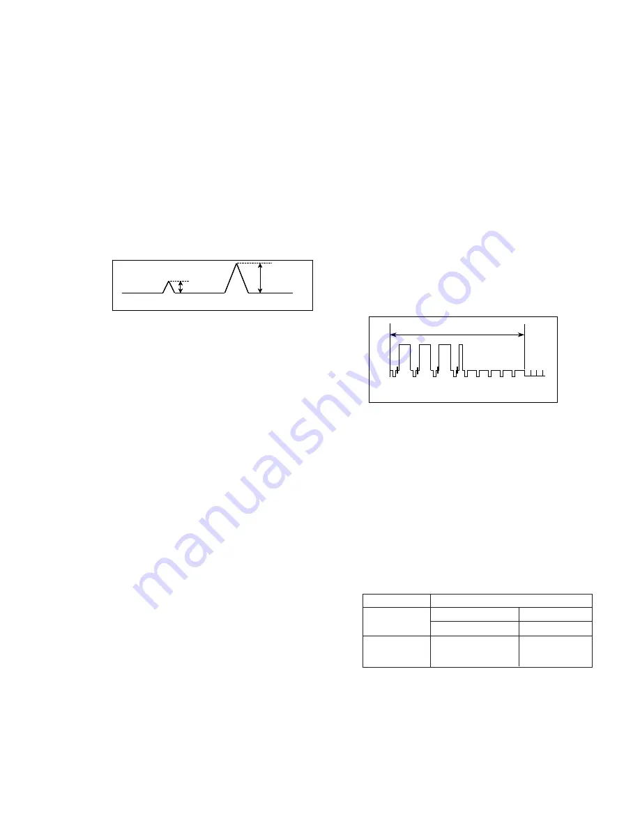
adjust CTL waveform to the following procedures.
A. If is over 2.5 :1, lower the head height.
After turning the height adjust screw counter-clockwise to
adjust its level from 1.5 : 1 to 2 : 1.
Check the tape location at P4. Readjust the TILT.(2:1)
B. If is under 1.5:1, heighten the head height.
After turning the height, adjust the screw clockwise to
adjust its level from 2 : 1 to 2.5 : 1.
Check the tape location of P4. Readjust the TILT.(2:1)
3. Play the standard tape and adjust very carefully the azimuth
screw right and left by using the oscilloscope and level-
meter to maximize the audio sound.
Adjust the azimuth screw & the height adjust screw at the
same time because they have mutual relationship. (Check
CTL again after the adjustment)
*A/C head adjustment order
Height adjust screw->check the TILT->azimuth screw
->check CTL
3.2.3 AUDIO LEVEL CHECKING AND ADJUSTMENT
1. Connect “+” terminal of RMS meter (auto level meter) to J108
on the main PCB Audio output and “-” terminal to GND.
2. Check that if audio level of RMS meter satisfies with the
spec,If audio sound is weak, adjust the A/C head azimuth
screw.
3. Audio level spec
1K :0.5
!
0.1Vrms
6K :1KHz
!
1.5dB
3.3. X-DISTANT/P2,P3 ADJUSTMENT
3.3.1. NECESSARY INSTRUMENT
1. SP PAL TAPE
2. OSCILLOSCOPE
3. 10:1 PROBE : 2 PIECES
4.SPEACIAL DRIVER FOR ADJUSTMENT(P2,P3,X-
DISTANT(NUT),AUDIO(NUT))
5. RMS METER(AUDIO LEVEL METER)
3.3.2. ADJUSTMENT PREPARATION
1.Connect oscilloscope(CH-1) to J123(H/SW) on main PCB.
(Use for trigger of CH-2 )
2.Connect oscilloscope(CH-2) to J158(RF) on main PCB.
(Use waveform of CH-2)
3. Play by inserting SP PAL TAPE. (2hd:normal tape)
4. After the picture is appeared, make initial condition by
pressing the tracking adjustment up(+) button of the remote
controller.
3.3.3. X-DISTANCE ADJUSTMENT
1. Turn the X-distant adjust groove of the deck right and left to
maximize the scope waveform.
2. Check that if waveform satisfies with the linearity by pressing
TRK Up(+) and Down(-) button.
3. Tighten the X-distant adjust screw.
3.3.4. P2/P3(RF LINEARITY) CHECK & ADJUSTMENT
1. Adjust p2 & p3 so that the the RF envelope waveform of the
oscilloscope becomes C in figure 2.
2. Check if the envelope waveform becomes maximum by
pressing TRK Up(+),Down(-) button onestep.
3.4. PG ADJUSTMENT
Adjust it after finishing controlling the Deck.
3.4.1.NECESSARY INSTRUMENT
1. SP PAL TAPE
2. OSCILLOSCOPE
3. 10 : 1 PROBE : 2 PIECES
3.4.2. ADJUSTMENT
1. Insert and play the SP PAL TAPE.
2. Connect the oscilloscope(CH-1) to H/SW(J123) on the main
PCB and trigger in setting the VOL/DIV to 1V range.
3. Connect the oscilloscope(CH-2) to video out(J173) on the
main PCB and set the VOL/DIV to 500mV range.
4. Set the TIME/DIV of oscilloscope to 50us range.
5. Adjust the falling edge(412us
!
20us) of vertical sync in the
video signal by varying VR01.
4.ASSEMBLY LINE ADJUSTMENT
4.1. RF AGC ADJ.( APPLYING THE W/S TUNER )
4.1.1. NECESSARY INSTRUMENT : DIGITAL MULTIMETER
4.1.2. ADJUSTMENT PREPARATION
1. HEAT-RUN at least 15 minutes before adjustment.
2. Input the PAL DIGITAL PATTERN(EU05); The intensity of
electric field for the applied tuner refers to the below data.
3. Connect the DIGITAL MULTIMETER to TP-AGC(J335) of
MAIN1.
4.1.3. ADJUSTMENT
1. Press the SVC key of the transmitter and select
¡
AGC
¡–
of the
SVC MENU using PR+/- key.
2. Adjust it by the below data varying VOL+/- key.
4.2. FOCUS ADJUSTMENT
4.2.1. Receive the standard color signal.
4.2.2. Let the picture be the most clear by the criterion of the
vertical line of it, varying the focus V/R of FBT.
1
2
CTL WAVEFORM
1
2
CTL WAVEFORM
1
2
CTL WAVEFORM
ADJUST PERIOD (6.5H = 412us)
PG ADJUST WAVEFORM
* CAUTION: SET THE TRIGGER MODE OF OSCILLOSCOPE TO DC
ADJUST PERIOD (6.5H = 412us)
PG ADJUST WAVEFORM
* CAUTION: SET THE TRIGGER MODE OF OSCILLOSCOPE TO DC
TUNER
6700VPF009V
6700VMF001H
6700VPF009Q
Electric fields strenth
AGC Voltage
AGC Voltage
70dBu
!
1dBu
2.7
!
0.05Vdc
AGC not adjust.
Setting & Adjustment
Summary of Contents for KE/KL-20/21P32X
Page 6: ...3 9 BLOCK DIAGRAM ...


