3. TECHNICAL BRIEF
- 53 -
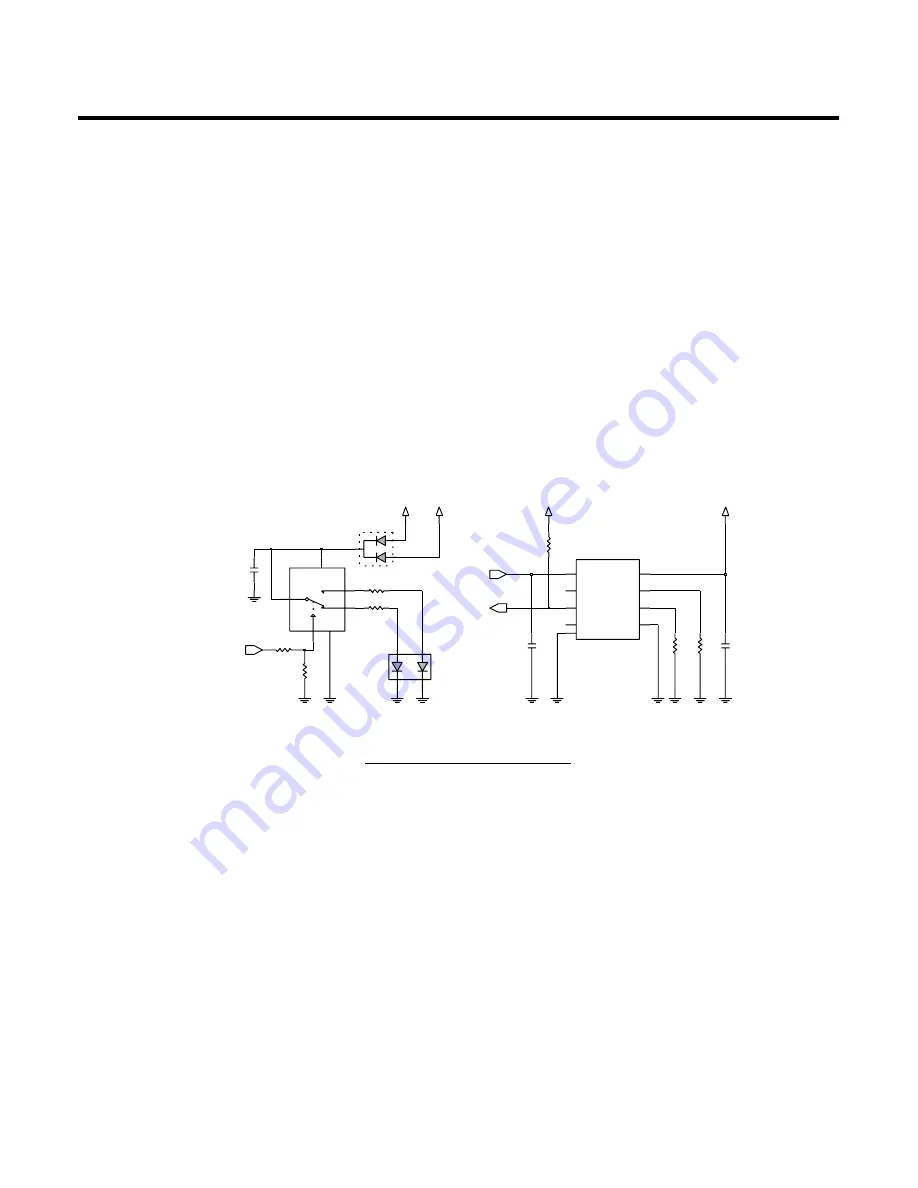
3.15. USB charging circuit
The USB charging circuit is a fully integrated USB VBUS voltage single-cell Li-ion battery charger
circuit.
The charger uses a CC/CV charge profile required by Li-ion batteries. CC charging current and End of
charging current is programmable I
REF
& I
MIN
resistors.
I
REF
resistor between this pin and the GND pin to set the charge current limit determined by the
following equation:
I
CC
= 12089/39K = 310mA
The End Of Charging current is set by IMIN That can be programmed by the as following equation:
I
EOC
= 11000/220K = 50mA
Charging indicator LED LD100 controlled by S-GOLD2’s GPIO that is CHG_LED_CTRL. When
TA(Travel Adaptor) is plugged in to 18pin MMI connector, SM-POWER detect charger voltage then
inform charger detecting to S-GOLD2. S-GOLD2 maintain low level of CHG_LED_CTRL until get
EOC(End Of Charging) message from SM-POWER. The LD100 controlled by S-GOLD2 both power
off and power on case. When USB cable is connected via MMI connector, indicator LED is controlled
same mechanism with TA inserted case. USB charging EOC is not indicated when the terminal is in off
status. LED just indicates charging status even though USB charging process reached EOC because
S_GOLD2 is in off status.
Figure 27 USB charging circuit
10K
R177
0.1u
C140
0.1u
C141
VCHG
220K
R141
39K
R142
0.1u
C168
U108
NLAST4599DFT2G
5
COM
GND
3
1
IN
NC
4
6
NO
2
VCC
VBAT
R178
1K
5
GND
IMIN
6
IREF
7
9
PGND
VIN
1
3
_CHG
_EN
4
2
_PPR
ISL6294
U104
8
BAT
47
R184
3
1
2
KDS121E
D1
2V72_IO
330
R131
VBUS_USB
R180
100K
LD100
SML-521MUWT86
1
2
3
4
CHG_LED_CTRL
VBUS_USB
_USB_EOC
Summary of Contents for KE820
Page 1: ...Service Manual Model KE820 Service Manual KE820 Date August 2006 Issue 1 0 ...
Page 3: ... 4 ...
Page 5: ... 6 ...
Page 46: ...3 TECHNICAL BRIEF 47 Figure 18 EN SET port control method ...
Page 69: ...4 PCB layout 70 Figure 45 Main PCB bottom Figure 46 Main PCB bottom placement ...
Page 70: ...4 PCB layout 71 Figure 47 Sub PCB top Figure 48 Sub PCB top placement ...
Page 71: ...4 PCB layout 72 Figure 49 Sub PCB bottom Figure 50 Sub PCB bottom placement ...
Page 114: ...6 Download S W upgrade 115 6 2 Download program user guide ...
Page 115: ... 116 6 Download S W upgrade ...
Page 116: ... 117 6 Download S W upgrade ...
Page 117: ... 118 6 Download S W upgrade ...
Page 124: ... 125 8 PCB LAYOUT ...
Page 125: ... 126 8 PCB LAYOUT ...
Page 126: ... 127 8 PCB LAYOUT ...
Page 127: ... 128 8 PCB LAYOUT ...
Page 141: ... 142 ...
Page 161: ...Note ...
Page 162: ...Note ...


