


LGE Internal Use Only
Copyright © 2008 LG Electronics. Inc. All right reserved.
Only for training and service purposes
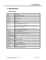
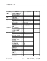
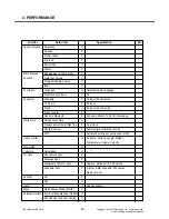
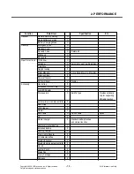
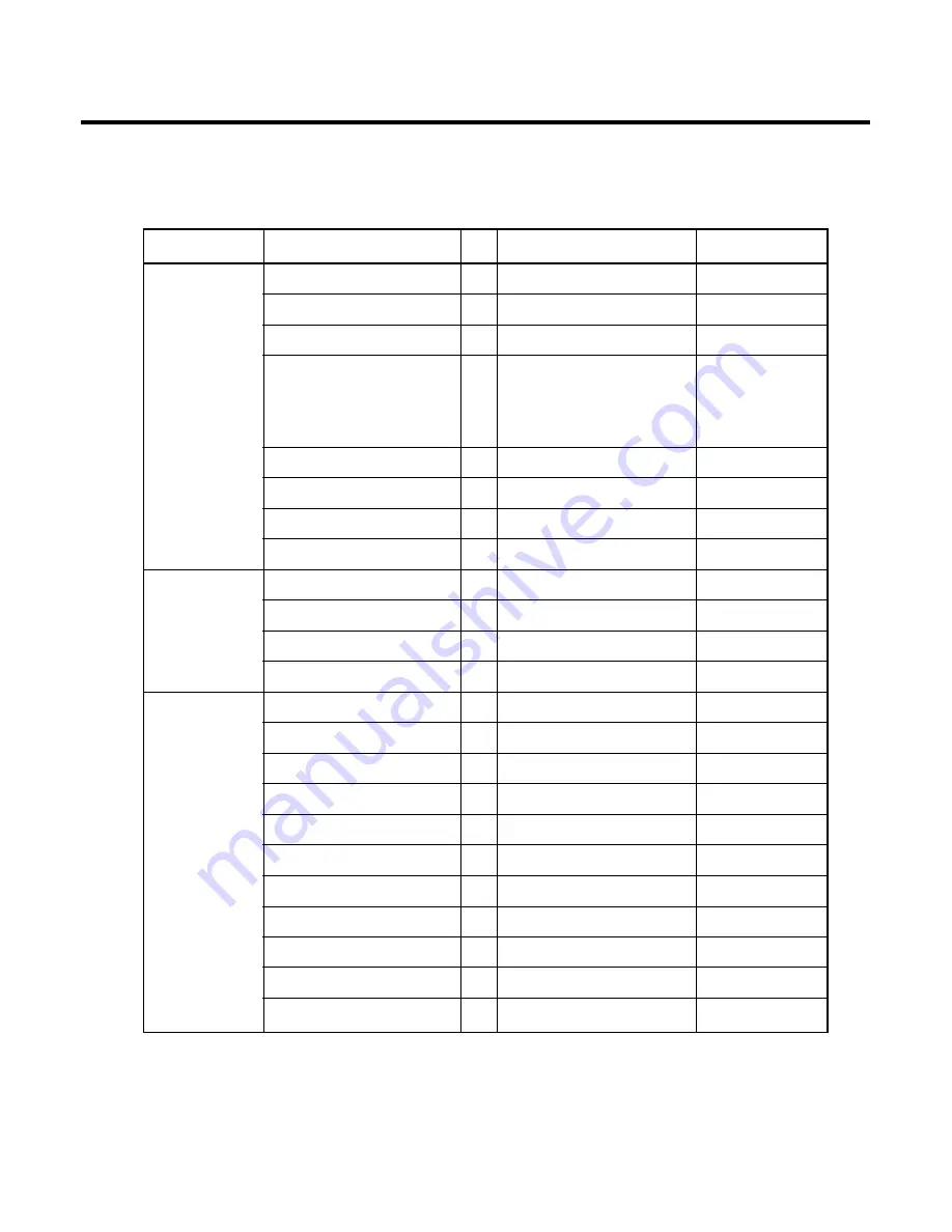
Function
Detail Item
Specification
Etc.
Display
RSSI
O
6 level
Battery Level
O
5 level
RTC
O
Multi Language
O
Basic:English
Max. 4 language of Latin
2 or 3 language of etc.
Quick Access Mode
X
PLMN/Service Indicator
O
Dimming Clock
X
Dual Clock
X
Local Time / Selected Area Time
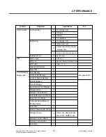
Normal Features
Last Dialed Number
O
20
Last Received Number
O
20
Last Missed Number
O
20
Scratch Pad Memory
X
Call
Call Waiting
O
Manage-ment
Call Swap
O
Call Retrieve
O
Auto Answer
X
Automatic Redial
O
Calling Line identification
O
Full Call divert
O
Speed Dialing
O
Last Number Redial
O
Multi-party Call (Conference Call)
O
Explicit Call Transfer
X
2. PERFORMANCE
- 9 -


