


담
당
관 리 자
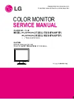
Model Description
MODEL
BRAND
Printing Specification
1. Trim Size (Format) :
215mm x 280 mm
2. Printing Colors
•
Cover :
LG COLORS
•
Inside :
Black
3. Stock (Paper)
•
Cover :
Snow White 150 g/
㎡
•
Inside :
Snow White 100 g/
㎡
4. Printing Method :
5. Bindery :
Saddle stitch
6. Language :
English
7. Number of pages :
28 (Including blank 1page)
Part No.
1.
2
.
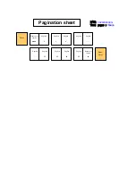
Service Guide Specification
Service Guide Specification
Changes
4.
REV.
NO.
MM/DD/YY
SIGNATURE
CHANGE NO.
CHANGE CONTENTS
1
2
3
4
5
7
6
SUFFIX
LEE H.J
05.11.02
L1732S-SFN
L1932S-SFN
LG
38289S0009Q
KIM J.O
05.11.02
(1) Origin Notification
* LGEDI : Printed in Indonesia
* LGEWA : Printed in U.K.
* LGESP : Printed in Brazil
* LGEMX : Printed in Mexico
* LGENT : Printed in China
* LGEIL : Printed in India
8
Special Instructions
3
.
Product Name
KNRUQPT
KXRUQPT
FLATRON L1732S
FLATRON L1932S


