


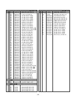


- 21 -
DATE: 2005. 11. 02.
*S
*AL LOC. NO.
PART NO.
DESCRIPTION / SPECIFICATION
C204
0CK104CK56A
0.1UF 1608 50V 10% R/TP X7R
C205
0CK104CK56A
0.1UF 1608 50V 10% R/TP X7R
C206
0CK104CK56A
0.1UF 1608 50V 10% R/TP X7R
C207
0CK104CK56A
0.1UF 1608 50V 10% R/TP X7R
C211
0CK103CK51A
0.01UF 1608 50V 10% R/TP B(Y
C213
0CK103CK51A
0.01UF 1608 50V 10% R/TP B(Y
C214
0CK103CK51A
0.01UF 1608 50V 10% R/TP B(Y
C215
0CK103CK51A
0.01UF 1608 50V 10% R/TP B(Y
C216
0CK103CK51A
0.01UF 1608 50V 10% R/TP B(Y
C217
0CK103CK51A
0.01UF 1608 50V 10% R/TP B(Y
C218
0CK103CK51A
0.01UF 1608 50V 10% R/TP B(Y
C219
0CK103CK51A
0.01UF 1608 50V 10% R/TP B(Y
C220
0CK103CK51A
0.01UF 1608 50V 10% R/TP B(Y
C221
0CK103CK51A
0.01UF 1608 50V 10% R/TP B(Y
C222
0CK103CK51A
0.01UF 1608 50V 10% R/TP B(Y
C223
0CK103CK51A
0.01UF 1608 50V 10% R/TP B(Y
C224
0CK103CK51A
0.01UF 1608 50V 10% R/TP B(Y
C225
0CK103CK51A
0.01UF 1608 50V 10% R/TP B(Y
C226
0CK103CK51A
0.01UF 1608 50V 10% R/TP B(Y
C230
0CK104CK56A
0.1UF 1608 50V 10% R/TP X7R
C231
0CK104CK56A
0.1UF 1608 50V 10% R/TP X7R
C232
0CK104CK56A
0.1UF 1608 50V 10% R/TP X7R
C233
0CK104CK56A
0.1UF 1608 50V 10% R/TP X7R
C240
0CK104CK56A
0.1UF 1608 50V 10% R/TP X7R
C251
0CK103CK51A
0.01UF 1608 50V 10% R/TP B(Y
C503
0CK103CK51A
0.01UF 1608 50V 10% R/TP B(Y
C504
0CH8106F611
10UF 16V M 85STD(CYL) R/TP
C506
0CC030CK01A
3PF 1608 50V 0.25 PF R/TP NP
C507
0CC180CK41A
18PF 1608 50V 5% R/TP NP0
C508
0CK103CK51A
0.01UF 1608 50V 10% R/TP B(Y
C701
0CK105CD56A
1UF 1608 10V 10% R/TP X7R
C707
0CC680CK41A
68PF 1608 50V 5% R/TP NP0
C708
0CK103CK51A
0.01UF 1608 50V 10% R/TP B(Y
C709
0CK103CK51A
0.01UF 1608 50V 10% R/TP B(Y
C717
0CC101CK41A
100PF 1608 50V 5% R/TP NP0
C718
0CC101CK41A
100PF 1608 50V 5% R/TP NP0
C727
0CK105CD56A
1UF 1608 10V 10% R/TP X7R
C732
0CK103CK51A
0.01UF 1608 50V 10% R/TP B(Y
C733
0CK104CK56A
0.1UF 1608 50V 10% R/TP X7R
C734
0CK104CK56A
0.1UF 1608 50V 10% R/TP X7R
C735
0CK104CK56A
0.1UF 1608 50V 10% R/TP X7R
C744
0CC680CK41A
68PF 1608 50V 5% R/TP NP0
C803
0CE107EF610
"100UF KMG,RD 16V 20% FL BULK"
C805
0CK104CK56A
0.1UF 1608 50V 10% R/TP X7R-L1732S
C809
0CK103CK51A
0.01UF 1608 50V 10% R/TP B(Y
C812
0CE107EF610
"100UF KMG,RD 16V 20% FL BULK"
C814
0CE107EF610
"100UF KMG,RD 16V 20% FL BULK"
C817
0CK105CD56A
1UF 1608 10V 10% R/TP X7R-L1932S
C818
0CC102CK41A
1000PF 1608 50V 5% R/TP NP0-L1932S
C819
0CK105CD56A
1UF 1608 10V 10% R/TP X7R
DATE: 2005. 11. 02.
*S
*AL LOC. NO.
PART NO.
DESCRIPTION / SPECIFICATION
D701
0DSIH00018A
"ENKMC2837-T112,LF ISAHAYA R/"
D702
0DSIH00018A
"ENKMC2837-T112,LF ISAHAYA R/"
D706
0DSIH00018A
"ENKMC2837-T112,LF ISAHAYA R/"
ZD701
0DZ560009GB
"BZT52C5V6S-(F),LF DIODES R/T"
ZD702
0DZ560009GB
"BZT52C5V6S-(F),LF DIODES R/T"
ZD703
0DZ560009GB
"BZT52C5V6S-(F),LF DIODES R/T"
ZD704
0DZ560009GB
"BZT52C5V6S-(F),LF DIODES R/T"
ZD711
0DZ560009GB
"BZT52C5V6S-(F),LF DIODES R/T"
ZD712
0DZ560009GB
"BZT52C5V6S-(F),LF DIODES R/T"
Q502
0IKE704200H
KIA7042AP TO-92 TP 4.2 VOLT.
U201
0IPRPM3017B
FE2040-LF(TSU16AWL) MSTAR 10
U501
0IZZ9H0047A
MTV412PMV MYSON PLCC 44PIN F-L1732S
U501
0IZZ9H0048A
MTV412PMV MYSON LQFP 44PIN F-L1932S
U502
0ICS240813B
"CAT24WC08J-TE13 8P,SOIC R/TP"
U801
0IPMGKE011A
KIA78D33F KEC DPAK R/TP 3.3V-L1932S
U802
0TFVI80067A
SI3865BDV(E3) VISHAY R/TP TS
Q503
0TRIH80001A
"RT1C3904-T112,LF ISAHAYA R/T"
Q504
0TRIH80001A
"RT1C3904-T112,LF ISAHAYA R/T"
Q505
0TRIH80001A
"RT1C3904-T112,LF ISAHAYA R/T"
Q703
0TR390609FA
FAIRCHILD KST3906-MTF TP SOT
Q704
0TR390609FA
FAIRCHILD KST3906-MTF TP SOT
Q801
0TR127309AA
KTA1273 TP KEC TO92 -Y(KTA96-L1732S
Q802
0TRIH80001A
"RT1C3904-T112,LF ISAHAYA R/T"-L1732S
Q803
0TR127309AA
KTA1273 TP KEC TO92 -Y(KTA96
R201
0RJ0682D677
68 OHM 1/10 W 5% 1608 R/TP
R202
0RJ0682D677
68 OHM 1/10 W 5% 1608 R/TP
R203
0RJ0682D677
68 OHM 1/10 W 5% 1608 R/TP
R207
0RJ3900D677
390 OHM 1/10 W 5% 1608 R/TP
R208
0RJ0682D677
68 OHM 1/10 W 5% 1608 R/TP
R209
0RJ0682D677
68 OHM 1/10 W 5% 1608 R/TP
R210
0RJ0682D677
68 OHM 1/10 W 5% 1608 R/TP
R216
0RJ0000D677
0 OHM 1/10 W 5% 1608 R/TP
R217
0RJ0000D677
0 OHM 1/10 W 5% 1608 R/TP
R220
0RJ4701D677
4.7K OHM 1/10 W 5% 1608 R/TP
R240
0RJ1001D677
1K OHM 1/10 W 5% 1608 R/TP
R501
0RJ4701D677
4.7K OHM 1/10 W 5% 1608 R/TP
R503
0RJ4701D677
4.7K OHM 1/10 W 5% 1608 R/TP
R506
0RJ4701D677
4.7K OHM 1/10 W 5% 1608 R/TP
R508
0RJ4701D677
4.7K OHM 1/10 W 5% 1608 R/TP
R520
0RJ4701D677
4.7K OHM 1/10 W 5% 1608 R/TP
R521
0RJ4701D677
4.7K OHM 1/10 W 5% 1608 R/TP
R522
0RJ4701D677
4.7K OHM 1/10 W 5% 1608 R/TP
R523
0RJ4701D677
4.7K OHM 1/10 W 5% 1608 R/TP
R530
0RJ1002D677
10K OHM 1/10 W 5% 1608 R/TP
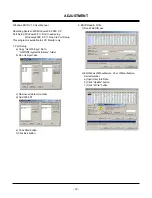
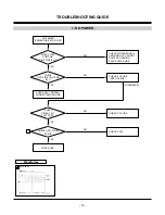
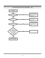
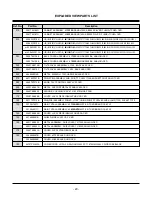
REPLACEMENT PARTS LIST
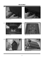
CAUTION: BEFORE REPLACING ANY OF THESE COMPONENTS,
READ CAREFULLY THE SAFETY PRECAUTIONS IN THIS MANUAL.
* NOTE : S
SAFETY Mark
AL ALTERNATIVE PARTS
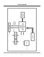
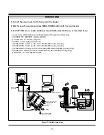
MAIN BOARD
CAPACITORS
DIODEs
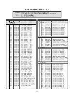
ICs
TRANSISTOR
RESISTORs


