


COLOR MONITOR
E-mail:http://www.LGservice.com/techsup.html
BEFORE SERVICING THE UNIT,
READ THE
xx:sales marketing, Mstar scaler, C
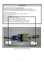
MSTAR Chip
.
Summary of Contents for L1734S
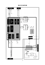
Page 11: ...11 BLOCK DIAGRAM TSUM1PFR h t t p w w w w j e l n e t ...
Page 23: ...23 WIRING DIAGRAM 89G 76J 8525 89G179J30N587 95G 825 7W503 h t t p w w w w j e l n e t ...
Page 24: ...24 EXPLODED VIEW h t t p w w w w j e l n e t ...
Page 41: ...Jan 2008 P NO Printed in China h t t p w w w w j e l n e t ...


