- 2-3 -
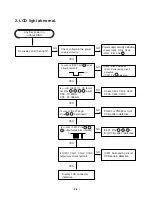
3. Initial reading is not carried out.
YES
YES
YES
YES
YES
YES
YES
YES
YES
YES
YES
YES
YES (with disc)
NO
NO
NO
NO
NO
NO
NO
NO
NO
NO
NO
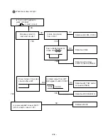
Slide motor moves.
(With disc)
Spindle motor turns.
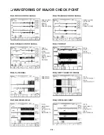
(Refer to FIG3.)
Does RF waveform
appear at IC506 Pin
(Refer to FIG4.)
Check the Voltage change of
PN502 Pin (6.4~6.8V).
Check the Voltage change of PN506
Pins , , , . (1.4V~1.8V).
Check the Data transmission
from IC510 pins , ,
(Refer to FIG7.)
Check the Data transmission
from IC510 pins , ,
(Refer to FIG8.)
Check the TRVP
Voltage.
(IC506 Pins )
Check the change of
SL +, SL – Voltage.
(IC504 Pins , )
Does FA+ waveform appear
at IC504 Pin ?
(Refer to FIG1.)
Laser light check A ?
Defective contact
PN501 or PICK-UP
Defective IC504
Defective IC506
Defective IC506
Defective MICOM
Defective IC506
Defective
Connector. (PN502)
Does TE waveform appear at
R517? (Refer to FIG2.)
Is rotation normal?
Is there no dropout of RF signal?
Defective IC506 or
PICK-UP
1
42
26
76
77
42
58
48
23
13
15
14
57
71
70 72
Summary of Contents for LAC-M5600
Page 11: ... 1 10 ...
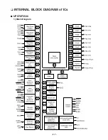
Page 18: ... 2 7 INTERNAL BLOCK DIAGRAM of ICs UPD78F0546 1 Block Diagram ...
Page 20: ... 2 9 2 Pin Descriptions ...
Page 21: ... 2 10 ...
Page 22: ... 2 11 BD3805F SCF built in sound processor 1 BLOCK DIAGRAM ...
Page 23: ... 2 12 HA13173 Multi Voltage Regulator IC ...
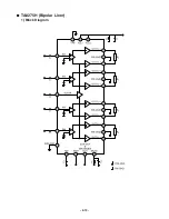
Page 24: ... 2 13 TA8275H Bipolar Liner 1 Block Diagram ...
Page 25: ... 2 14 AM5810 Motor Driver IC 1 Block Diagram ...
Page 26: ... 2 15 3 Pin Function ...
Page 32: ... BLOCK DIAGRAM WHOLE 2 21 2 22 ...
Page 33: ...2 23 2 24 BLOCK DIAGRAM CDP ...
Page 34: ...2 25 2 26 SCHEMATIC DIAGRAMS MAIN SCHEMATIC DIAGRAM ...
Page 35: ...2 27 2 28 FRONT SCHEMATIC DIAGRAM ...
Page 36: ...2 29 2 30 USB SCHEMATIC DIAGRAM ...
Page 37: ...2 31 2 32 USB SUB SCHEMATIC DIAGRAM ...
Page 38: ...2 33 2 34 CD SCHEMATIC DIAGRAM ...
Page 39: ...2 35 2 36 PRINTED CIRCUIT BOARD DIAGRAMS MAIN P C BOARD DIAGRAM BOTTOM ...
Page 41: ...2 39 2 40 CD P C BOARD BOTTOM CD P C BOARD TOP ...


