- 2-19 -
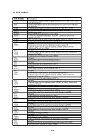
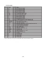
3) Pin Function
Pin no.
Symbol
I/O
Function
1
A11
O
Adress signal output for DRAM11
2
A9
O
Adress signal output for DRAM9
3
A8
O
Adress signal output for DRAM8
4
A7
O
Adress signal output for DRAM7
5
A6
O
Adress signal output for DRAM6
6
A5
O
Adress signal output for DRAM5
7
A4
O
Adress signal output for DRAM4
8
NWE
O
Writing enable signal output for DRAM
9
NCAS
O
CAS control signal output for DRAM
10
NRAS
O
RAS control signal output for DRAM
11
A3
O
Adress signal output for DRAM3
12
A2
O
Adeess signal output for DRAM2
13
A1
O
Adress signal output for DRAM11
14
A0
O
Adress signal output for DRAM0
15
A10
O
Adress signal output for DRAM10
16
*BA0
I/O
Bank Selection signal output for SDRAM 0/Monitor serial input
17
*BA1
I/O
Bank Selection signal output for SDRAM 1/Monitor serial input
18
PRAMVSS33
I
GND for built-in DRAM
19
PRAMVDD33
I
Power supply input for built-in DRAM
20
PRAMVDD15
–
Power supply output for built-in DRAM 1.6V
21
SPOUT
O
Power supply for digital circuits
22
*PC
I/O
Spindle motor drive signal output (Absolute value output)/Monitor serial input
23
TRVP
O
Traverse drive signal output (positive polarity)
24
TRP
O
Tracking drive signal output (positive polarity)
25
FOP
O
Focus drive signal output (positive polarity)
26
DVSS1
I
Ground 1 for digital circuits
27
IOVDD2
I
Power supply 2 for digital I/O
28
DVDD1
–
Power supply 1 for internal digital circuits
29
SRVMON0
O
Servo Monitor Output
30
SRVMON1
O
Servo Monitor Output
31
AVSS2
I
Analog circuit VSS (For DSL, PLL, AD, RF)
32
OSCIN
I
Servo Disturbance Input
33
CTRCRS
O
Tracking coss comparator output
34
VREF
O
VREF output
35
E
I
Tracking signal input 1
36
F
I
Tracking signal input 2
37
D
I
Focus signal input4
38
B
I
Focus signal input2
39
C
I
Focus signal input3
40
A
I
Focus signal input1
Note) pins marked with an asterisk can be switched to different signals by using microcontroller commands.
Summary of Contents for LAC-M7600
Page 12: ... 2 7 INTERNAL BLOCK DIAGRAM of ICs FRONT 1 MICOM PIN Assignment ...
Page 13: ... 2 8 2 Pin Descriptions ...
Page 14: ... 2 9 ...
Page 15: ... 2 10 3 Pin Descriptions ...
Page 17: ... 2 12 78K0 KF2 1 Block Diagram ...
Page 19: ... 2 14 3 Pin Function ...
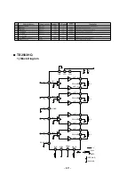
Page 20: ... 2 15 AM5810 1 Block Diagram ...
Page 21: ... 2 16 3 Pin Function ...
Page 26: ... BLOCK DIAGRAM 2 21 2 22 ...
Page 27: ...2 23 2 24 SCHEMATIC DIAGRAMS MAIN SCHEMATIC DIAGRAM ...
Page 28: ...2 25 2 26 MAIN 2 SCHEMATIC DIAGRAM ...
Page 29: ...2 27 2 28 MAIN 3 SCHEMATIC DIAGRAM ...
Page 30: ...2 29 2 30 MAIN 4 SCHEMATIC DIAGRAM ...
Page 31: ...2 31 2 32 FRONT SCHEMATIC DIAGRAM ...
Page 32: ...2 33 2 34 CD SCHEMATIC DIAGRAM ...
Page 33: ...2 35 2 36 TRIM SCHEMATIC DIAGRAM ...
Page 34: ...2 37 2 38 PRINTED CIRCUIT BOARD DIAGRAMS MAIN P C BOARD DIAGRAM ...
Page 35: ...2 39 2 40 MAIN P C BOARD DIAGRAM ...
Page 36: ...2 41 2 42 FRONT TRIM P C BOARD DIAGRAM TRIM P C BOARD ...
Page 37: ...2 43 2 44 CD P C BOARD ...

