background image

2-6

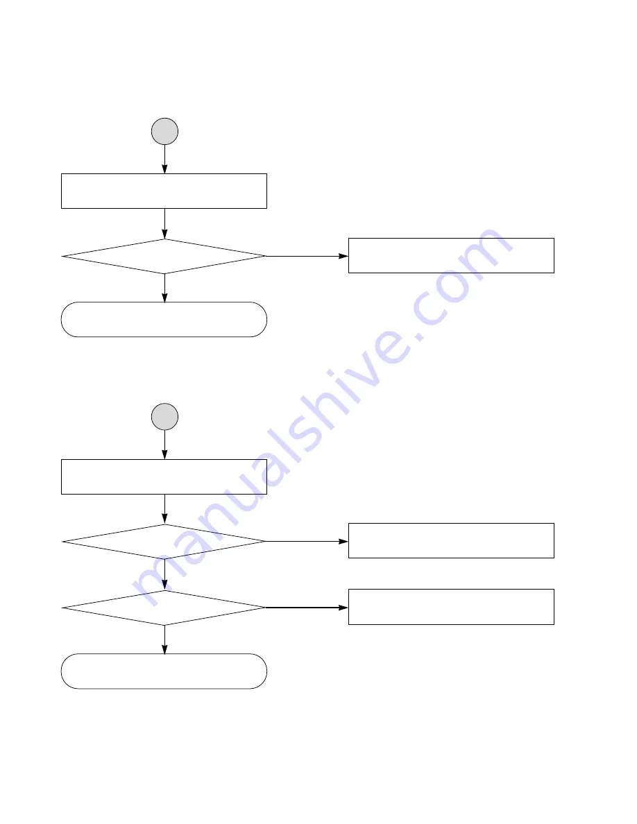
CD no sound?

OK

YES

IC520(1, 2, 3)

YES

NO

Fig 8

Fig 3, 4

Checked the DAC signal in?

B

No ejected the CD?

OK

YES

CN901(16) [MAIN]

YES

NO

Checked the Eject key?

YES

D6, D5

NO

Checked the loading motor

control?

C

Copyright © 2007 LG Electronics. Inc. All right reserved.

Only for training and service purposes

LGE Internal Use Only

Summary of Contents for LAC6700R

Page 1: ...IVER SERVICE MANUAL MODEL LAC6700R CAUTION BEFORE SERVICING THE UNIT READ THE SAFETY PRECAUTIONS IN THIS MANUAL MODEL LAC6700R SERVICE MANUAL P NO AFN35097871 OCTOBER 2007 Website http biz lgservice com Internal Use Only ...

Page 2: ... 7 IC801 TB2904HQ 2 20 8 IC901 LD3811 2 21 BLOCK DIAGRAM 2 23 CIRCUIT DIAGRAMS 2 25 1 MAIN CIRCUIT DIAGRAM 2 25 2 CDP 1 CIRCUIT DIAGRAM 2 27 3 CDP 2 CIRCUIT DIAGRAM 2 29 4 FRONT CIRCUIT DIAGRAM 2 31 5 USB CIRCUIT DIAGRAM 2 33 6 LCD LIGHTING CIRCUIT DIAGRAM 2 34 PRINTED CIRCUIT DIAGRAMS 2 35 1 MAIN P C BOARD 2 35 2 CDP P C BOARD 2 39 3 FRONT P C BOARD 2 40 4 USB P C BOARD 2 41 5 LCD LIGHTING P C BO...

Page 3: ...precautions are indicated or printed on the cabinet chassis or components When servicing follow the printed or indicated service precautions and service materials 2 The Components used in the unit have a specified conflammability and dielectric strength When replacing any components use components which have the same ratings Components marked in the circuit diagram are important for safety or for ...

Page 4: ...n propelled chemicals These can generate electrical charges sufficient to damage ESD devices 6 Do not remove a replacement ESD device from its protective package until immediately before you are ready to install it Most replacement ESD devices are packaged with leads electrically shorted together by conductive foam aluminum foil or comparable conductive materials 7 Immediately before removing the ...

Page 5: ... 20kHz S N Ratio 85dB Distortion 0 05 Channel Separation 1kHz 60dB RADIO SECTION FM Frequency Range 65 74 87 5 107 9 or 87 5 108MHz S N Ratio 53dB Distortion 0 7 Usable Sensitivity 12dBµV AM MW Frequency Range 520 1720 or 522 1620kHz S N Ratio 45dB Distortion 1 0 Usable Sensitivity 28dBµV USB SECTION Version USB 1 1 Copyright 2007 LG Electronics Inc All right reserved Only for training and service...

Page 6: ...r IC Control IC801 4 22 IC401 3 10 Checked the Power IC Signal in out IC801 11 12 14 15 IC801 3 5 7 9 17 19 21 23 Checked the Power IC Mute IC801 22 Checked the Power IC Standby IC801 4 Checked the Power IC Ripple IC801 10 Checked the Main Connector CN801 1 2 3 4 8 9 12 13 6 No Line out signal Checked the E VR Vdd IC301 10 IC601 24 Checked the E VR Ground IC601 15 Checked the E VR control IC601 22...

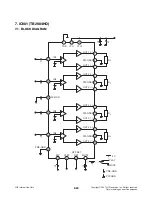
Page 7: ...anged IC We request that you send it to HQ RL RL RL 11 9 8 7 5 2 3 17 18 19 21 24 23 12 15 14 1 20 6 RL IN1 IN2 IN3 IN4 13 C1 C1 C1 C1 PRE GND 10 25 22 OUT1 PW GND1 OUT1 OUT2 PW GND2 OUT2 OUT3 PW GND3 OUT3 OUT4 PW GND4 OUT4 TAB VCC1 VCC2 C 3 C 4 C 2 PRE GND PW GND STBY RIP MUTE C 5 16 C6 4 OFF SET DET MUTE PLAY 5 V R1 AC GND Stand by Power Sound Voltage ON OFF OFF 0 to 1 5 OFF ON ON 3 5 to 6V Mute...

Page 8: ... Vdd IC301 4 9 IC401 64 Checked the LED LD901 LD921 5 Don t moved Level bar Checked the Level Meter control IC601 25 26 IC401 9 54 6 Not avaliable to Dimmer control Chekced the Dimmer control CN801 11 Q303 Q304 IC301 4 9 No Symptom Check Point Location No TUNER FUNCTION 1 Not available to Tuner Checked the Tuner Vdd TU101 4 16 IC301 10 IC401 39 Q350 Q351 Checked the Tuner Ground TU101 3 5 10 17 Ch...

Page 9: ...72 YES NO Checked the CD DSP reset X503 YES NO Checked the CD DSP X tal PN504 3 YES NO Fig 3 4 Fig 1 2 Fig 1 2 Checked the disc in load switch CN510 12 17 IC513 12 14 15 YES NO Checked the loading motor control PN504 1 YES NO Checked the 8 12cm sens switch 2 CD PART TROUBLESHOOTING A B C Copyright 2007 LG Electronics Inc All right reserved Only for training and service purposes LGE Internal Use On...

Page 10: ...ontrol IC506 25 IC513 17 18 YES NO Checked the focus control IC506 25 R517 YES NO Checked the focus error level out FE mon IC506 54 YES NO Checked the PLL locking FSEQ IC506 41 16 YES NO Checked the RF signal out check IC506 21 IC513 8 5 YES NO Checked the spindle motor control PN504 5 6 YES NO Checked the TRVP control IC506 24 IC513 19 20 YES NO Checked the tracking control A Copyright 2007 LG El...

Page 11: ...Checked the DAC signal in B No ejected the CD OK YES CN901 16 MAIN YES NO Checked the Eject key YES D6 D5 NO Checked the loading motor control C Copyright 2007 LG Electronics Inc All right reserved Only for training and service purposes LGE Internal Use Only ...

Page 12: ...0 31 YES NO Checked the USB interface IC reset X505 YES NO Checked the USB interface IC X tal IC511 65 YES NO Fig 14 Checked the Flash memory option port IC511 62 63 YES NO Checked the D D port IC511 27 YES NO Checked the USB indication port IC506 62 63 64 YES NO Checked the USB interface IC control 3 USB PART TROUBLESHOOTING D YES Copyright 2007 LG Electronics Inc All right reserved Only for trai...

Page 13: ...cked the CD DSP X tal IC506 67 68 69 70 71 72 73 YES NO Fig 10 12 Checked the CD DSP control IC511 22 23 IC510 50 51 YES NO Checked the USB data D YES USB no sound IC520 1 2 3 YES NO Fig 8 Checked the CD DSP signal out YES YES Copyright 2007 LG Electronics Inc All right reserved Only for training and service purposes LGE Internal Use Only ...

Page 14: ...EW FEW SLED CON LOADING IN PIN504 PIN5 PIN504 PIN6 R5091 SLED CON R5465 LOAD IN SL SL SLED CON LOADING IN Fig 4 Motor control signal for unloading REW FEW SLED CON LOADING IN PIN504 PIN5 PIN504 PIN6 R5091 SLED CON R5465 LOAD IN SL SL SLED CON LOADING IN D6 REW D5 FEW R5091 SLED CON R5465 LOAD IN D6 REW D5 FEW R5091 SLED CON R5465 LOAD IN Copyright 2007 LG Electronics Inc All right reserved Only fo...

Page 15: ...l Fig 8 LRCK BCK DATA from DAC PLLF SP SP SPOUT IC520 PIN1 IC520 PIN2 IC520 PIN3 BCK DATA LRCK Fig 9 PD RFOUT Fig 10 CLK REQ DATA PD MD RFOUT LOADING IN IC511 PIN52 IC511 REQ PIN53 IC511 DATA PIN54 CLK REQ DATA IC506 PLLF PIN54 PN504 SP PIN7 PN504 SP PIN8 IC506 SPOUT PIN21 IC506 PD41 IC506 RFOUT46 Copyright 2007 LG Electronics Inc All right reserved Only for training and service purposes LGE Inter...

Page 16: ...NRST MDATA Fig 13 SLED control SL SL SL TRVP IC510 NRST PIN57 IC510 STAT PIN71 IC510 MDATA PIN48 Fig 14 USB D D signal D D UART RX UART TX PN503 PIN3 D PN503 PIN2 D R560 UART RX R562 UART TX IC510 MLD PIN58 IC510 MCLK PIN70 IC510 MDATA PIN72 R504 PIN5 PN504 PIN6 R5091 SLED CON R5465 LOAD IN Copyright 2007 LG Electronics Inc All right reserved Only for training and service purposes LGE Internal Use...

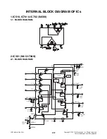
Page 17: ... DSPOUT CTL 2 2 5V CTL 3 2 5V CTL 4 2 5V 15 FREG F RFREG3 FREG B 13 12 11 10 9 8 7 6 5 4 3 2 1 14 3 5V DBUP CBUP 100uF CVDD 10uF CDSP 10uF CAUDIO 10uF CCD 0 1uF CEXT 10uF CILM 0 1uF CFREG 10uF QFREG RFREG1 RFREG2 DEXT1 DEXT2 C1 100uF C2 0 1uF 2 IC301 HA13173AH 2 1 BLOCK DIAGRAM Copyright 2007 LG Electronics Inc All right reserved Only for training and service purposes LGE Internal Use Only ...

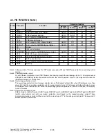
Page 18: ...ts except VDD pin14 and FREG pin2 3 are switched off when the circuit operates revert to the original state when the temperature drops to a certain level Note3 Overvoltage protection circuit The overvoltage protection circuit surge protector turns off all outputs without Vdd when VB voltage is more than about 21V And the overvoltage protection circuit surge protector turns off Vdd output with othe...

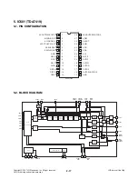
Page 19: ...CLK O PCDP_DI I PCDP_DO O PFRT_RST O PFRT_OPEN I PFRT_DETECT I PART_TX O PART_RX I PART_EN I PSD_ST I PPLL_CE O PEEPROM_CE O PDIM_IN I PRDS_DI I PPWR O PREMOTE O PTEL_MUTE I PAUDIO_MUTE O PAUX_MUTE O PLIGHT O PDIM_OUT O PEJECT I PQUALTY I PSMETER I PLEVEL_METER I PKEY2 I PKEY1 I AVss PEV_CLK O PEV_CE O PPWR_MUTE O PAF_MUTE O PRMC I PSOFT_MUTE O PEALA_SW1 O PEALA_SW2 O PSPEC_CLK O PSTANDBY O PDECK_...

Page 20: ...SB Flash upgrade enable 27 P86 EX6 PUSB_POWER PBT I O O CMOS USB power on BT power on 3 3V Ctrl 28 P87 EX7 PUSB_SW I O I USB device detect sw 29 P30 INTP3 RTC1HZ PUSB_RESET I O O CMOS OTG reset 30 EVDD1 Positive power supply for ports 31 P50 EX8 PUSB_PROTECT I O I Protection IC overcurrent detection 32 P51 EX9 POPT_IN0 I O For diode option check signal 1 or 2 input0 33 P52 EX10 POPT_IN1 I O I For ...

Page 21: ...TO07 PFRT_RST I O O CMOS Front micom LCD drv reset 76 P144 SO20 TxD2 PCDP_DO I O O CMOS Data output for CDP 77 P143 SI20 RxD2 SDA2 PCDP_DI I O I Data input for CDP 78 P142 SCK20 SCL2 PCDP_CLK I O O CMOS CLK output for CDP 79 P141 PCLBUZ1 INTP7 PFRT_CE I O I Data enable output to front micom LCD drv 80 P140 PCLBUZ0 INTP6 PBEEP I O O CMOS Buzzer output 81 P120 INTP0 EXLVI PEXLVI I O I Low voltage de...

Page 22: ...Softstep MonoFader Subwoofer LPF Mix Mix MIX OUTSW OUTRR2 HPF HPF Softstep MonoFader Softstep MonoFader AC2INL SE3L AC2INR SE3R ACOUTL AC2OUTL ACOUTR AC2OUTR ACINL FILOL ACINR FILOR VREFOUTF SAOUT SACLK InGain OUTLF OUTRF OUTLR OUTRR INPUT MULTIPLEXER InGain AutoZero I2 C BUS DIGITAL CONTROL I2 C BUS DIGITAL CONTROL OUTSW OUTLR2 MUTE Loudness Middle Treble Bass SoftMute Softstep Volume Softstep Mo...

Page 23: ... channel I 10 SE1R Single ended input 1 Right channel I 11 DIFFL Pseudo differential stereo input left I 12 DIFFG Pseudo differential stereo input common I 13 DIFFR Pseudo differential stereo input right I 14 CREF Reference capacitor O 15 GND Ground S 16 OUTSW OUTLR2 Subwoofer output 2nd rear left output O 17 OUTRF Front right output O 18 OUTRR Rear right output O 19 OUTLR Rear left output O 20 OU...

Page 24: ...FILR 9 BASSVROUT 21 ROUT 10 ealaVRIN 22 LOUT 11 ealaVROUT 23 RIN 12 GND 24 LIN 4 6 5 1 2 3 7 8 10 9 11 12 6 2 BLOCK DIAGRAM H eala_Bass H eala L BYPASS H L L H H L 1 50K 50K 3D FILTER LPF 2 3 4 5 11 12 16 17 18 19 20 21 22 Vref 50K 50K 14 15 13 23 24 9 10 8 6 7 VC HP HP H L L BYPASS SW SW SW SW SW SW Copyright 2007 LG Electronics Inc All right reserved Only for training and service purposes LGE In...

Page 25: ...3 C1 C1 C1 C1 PRE GND 10 25 22 OUT1 PW GND1 OUT1 OUT2 PW GND2 OUT2 OUT3 PW GND3 OUT3 OUT4 PW GND4 OUT4 TAB VCC1 VCC2 C 3 C 4 C 2 PRE GND PW GND STBY RIP MUTE C 5 16 C6 4 OFF SET DET MUTE PLAY 5 V R1 AC GND Copyright 2007 LG Electronics Inc All right reserved Only for training and service purposes LGE Internal Use Only ...

Page 26: ...EG19 SEG20 SEG21 SEG22 SEG23 SEG24 COM4 COM3 COM2 COM1 VDD VLCD VLCD1 VLCD2 VLCD3 VSS OSCO OSC1 RES CE CL DI 8 2 BLOCK DIAGRAM SEG60 COM9 SEG59 COM10 SEG58 SEG1 COM1 COMMON DRIVER INSTRUCTION DECODER SEGMENT DRIVER LATCH ADRAM 6 0 bits CGRAM 5X9X16 bits CGRAM 5X9X240 bits DCRAM 48X240 bits ADDRESS COUNTER ADDRESS REGISTER SHIFT REGISTER CCB INTERFACE TIMING GENERATOR CLOCK GENERATOR RES INSTRUCTIO...

Page 27: ...OM1 to COM8 L VSS Serial data transfer is disabled The OSCI OSCO pin oscillator is stopped When RES is high VDD Display on after a ìdisplay on off controlî display on state setting instruction is executed Serial data transfers are enabled The OSCI OSCO pin oscillator operates Used for applying the LCD drive 3 4 bias voltage externally Used for applying the LCD drive 2 4 bias voltage externally Use...

Page 28: ...2 23 2 24 BLOCK DIAGRAM Copyright 2007 LG Electronics Inc All right reserved Only for training and service purposes LGE Internal Use Only ...

Page 29: ...2 25 2 26 CIRCUIT DIAGRAMS 1 MAIN CIRCUIT DIAGRAM Copyright 2007 LG Electronics Inc All right reserved Only for training and service purposes LGE Internal Use Only ...

Page 30: ...2 27 2 28 2 CDP 1 CIRCUIT DIAGRAM Copyright 2007 LG Electronics Inc All right reserved Only for training and service purposes LGE Internal Use Only ...

Page 31: ...2 29 2 30 3 CDP 2 CIRCUIT DIAGRAM Copyright 2007 LG Electronics Inc All right reserved Only for training and service purposes LGE Internal Use Only ...

Page 32: ...2 31 2 32 4 FRONT CIRCUIT DIAGRAM Copyright 2007 LG Electronics Inc All right reserved Only for training and service purposes LGE Internal Use Only ...

Page 33: ...2 33 2 34 5 USB CIRCUIT DIAGRAM 6 LCD LIGHTING CIRCUIT DIAGRAM Copyright 2007 LG Electronics Inc All right reserved Only for training and service purposes LGE Internal Use Only ...

Page 34: ...2 35 2 36 1 MAIN P C BOARD TOP VIEW PRINTED CIRCUIT BOARD DIAGRAMS Copyright 2007 LG Electronics Inc All right reserved Only for training and service purposes LGE Internal Use Only ...

Page 35: ...2 37 2 38 MAIN P C BOARD BOTTOM VIEW Copyright 2007 LG Electronics Inc All right reserved Only for training and service purposes LGE Internal Use Only ...

Page 36: ...2 39 2 40 2 CDP P C BOARD 3 FRONT P C BOARD TOP VIEW BOTTOM VIEW Copyright 2007 LG Electronics Inc All right reserved Only for training and service purposes LGE Internal Use Only ...

Page 37: ...2 41 2 42 4 USB P C BOARD TOP VIEW BOTTOM VIEW 5 LCD LIGHTING P C BOARD Copyright 2007 LG Electronics Inc All right reserved Only for training and service purposes LGE Internal Use Only ...

Page 38: ...7 252 258 254 257 288 251 457 299 255 256 283 276 260 279 282 281 277 A45 A50 A43 A42 262 263 264 278 453 A49 A44 280 LCD901 CDP MAIN FRONT 450 296 458 458 250 259 289 269 267 266 274 268 265 275 286 273 271 272 270 Copyright 2007 LG Electronics Inc All right reserved Only for training and service purposes LGE Internal Use Only Accessory Loc No Loc No Loc No Loc No Loc No Loc No 835 801 808 818 85...

Page 39: ...2 3 4 5 1 1 2 2 MECHANISM PICK UP SECTION 3 3 3 4 Copyright 2007 LG Electronics Inc All right reserved Only for training and service purposes LGE Internal Use Only A03 ...

Reviews: