background image

SERVICE MANUAL

SERVICE MANUAL

CAUTION

BEFORE SERVICING THE UNIT, READ THE “SAFETY PRECAUTIONS”
IN THIS MANUAL.

Internal Use Only

Website http://biz.lgservice.com

FEBRUARY, 2015

MODEL: LAS350B (LAS350B, S35A1-W)

MODEL: LAS350B

(LAS350B, S35A1-W)


2.1 ch Sound Bar

P/NO : AFN77152011

Summary of Contents for LAS350B
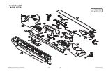
Page 1: ...AUTION BEFORE SERVICING THE UNIT READ THE SAFETY PRECAUTIONS IN THIS MANUAL Internal Use Only Website http biz lgservice com FEBRUARY 2015 MODEL LAS350B LAS350B S35A1 W MODEL LAS350B LAS350B S35A1 W 2 1 ch Sound Bar P NO AFN77152011 ...

Page 2: ...1 1 CONTENTS SECTION 1 GENERAL SECTION 2 CABINET MAIN CHASSIS SECTION 3 ELECTRICAL SECTION 4 REPLACEMENT PARTS LIST ...

Page 3: ...1 2 SECTION 1 GENERAL CONTENTS ESD PRECAUTIONS 1 3 HIDDEN KEY MODE 1 4 SERVICE INFORMATION FOR EEPROM 1 4 MCS EQ HIDDEN KEY GUIDE 1 5 MCS EQ PROGRAM UPDATE GUIDE 1 5 SPECIFICATIONS 1 6 ...

Page 4: ...harges sufficient to damage ESD devices 5 Do not use freon propelled chemicals These can generate electrical charges sufficient to damage ESD devices 6 Do not remove a replacement ESD device from its protective package until immediately before you are ready to install it Most replacement ESD devices are packaged with leads electrically shorted together by conductive foam aluminum foil or comparabl...

Page 5: ...ERSION CHECK Main set Volume Remote control LG TV up Sound Effect down NIGHT right F Skip Right left B Skip Left enter AV Sync OPT Status VFD OPT POWER ON Main set Volume Remote control OPTICAL Use arrow key Sound Effect NIGHT F Skip Right B Skip Left to move to appropriate position and make changes Remote control AV SYNC Display VFD E2P CLR Power off automatically Power cord unplug SERVICE INFORM...

Page 6: ...ly 5 Power cord unplug MCS EQ HIDDEN KEY GUIDE 1 Preparation Remote control Do format USB Memory to FAT32 File system USB Update file exist only in the USB Memory stick Ex LAS350B MCS E LAS350B_FW_201412221 bin if USB driver is E EQ E EQ_PRG_LAS350B_141219_0_4112 bin if USB driver is E 2 Update 1 Power on 2 Change the USB function Main set Volume Remote control MUTE 3 Insert USB 4 Display in VFD M...

Page 7: ...TPUT OPT IN 3 V p p Optical jack x 1 PORT IN 0 5 Vrms 3 5 mm stereo jack x 1 Available Digital Input Audio Sampling Frequency 32 kHz 44 1 kHz 48 kHz 96 kHz AMPLIFIER Total 120 W Front 25 W x 2 6 Ω at 1 kHz Subwoofer 70 W 4 Ω at 100 Hz THD 10 SUBWOOFER S35A1 W Type 1 Way 1 Speaker Impedance 4 Ω Rated Input Power 70 W Max Input Power 140 W Dimensions W x H x D 156 mm x 300 mm x 288 mm 6 1 inch x 11 ...

Page 8: ...2 1 SECTION 2 CABINET MAIN CHASSIS CONTENTS EXPLODED VIEWS 2 3 1 MAIN SET SECTION 2 3 2 SUBWOOFER SECTION 2 5 3 PACKING ACCESSORY SECTION 2 7 ...

Page 9: ...2 2 ...

Page 10: ...59 A52 264 504 K 300 USB DISPLAY MAIN SMPS B I G H A B E F H C D F G E J J A K I CABLE2 CABLE1 CABLE4 A47 505 504 A43 A46 505 505 A48 A55 265 256 256 EXPLODED VIEWS 1 MAIN SET SECTION NOTES THE EXCLAMATION POINT WITHIN AN EQUILATERAL TRIANGLE IS INTENDED TO ALERT THE SERVICE PERSONNEL TO THE PRESENCE OF IMPORTANT SAFETY INFORMATION IN SERVICE LITERATURE ...

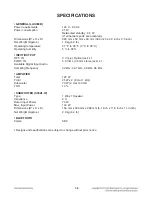
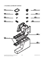
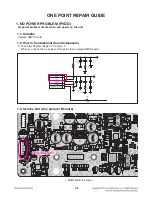
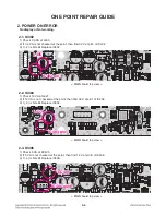
Page 11: ...A900 2 SUBWOOFER SECTION ...

Page 12: ...801 Owner s manual 835 Wall bracket 806 Optical cable 836 Screws 808 Batteries 837 Cover foot 900 Remote control 826 Filter Ferrite Core 803 Packing Main 802 Box 804 Bag 3 PACKING ACCESSORY SECTION ...

Page 13: ...2 8 ...

Page 14: ...SH MEMORY 3 15 3 TACT KEY 3 16 4 USB 3 17 5 REMOTE CONTROL 3 18 6 OPTICAL 3 19 7 PORTABLE 3 20 8 AUDIO PWM 3 21 9 AUDIO AMP 3 23 WIRING DIAGRAM 3 25 BLOCK DIAGRAM 3 27 CIRCUIT DIAGRAMS 3 29 1 SMPS CIRCUIT DIAGRAM 3 29 2 MAIN DSP CIRCUIT DIAGRAM 3 31 3 MAIN POWER CIRCUIT DIAGRAM 3 33 4 MAIN PWM AMP CIRCUIT DIAGRAM 3 35 5 DISPLAY KEY USB CIRCUIT DIAGRAM 3 37 CIRCUIT VOLTAGE CHART 3 39 PRINTED CIRCUI...

Page 15: ...power on the unit 1 1 Solution Replace SMPS board 1 2 How to troubleshoot Countermeasure 1 Check the PVDD voltage 32 V at pin1 2 When you check the no power at this point then replace SMPS board 1 3 Service hint Any picture Remark MAIN board top view R463 1K CON402 pin1 2 CON402 pin1 2 ...

Page 16: ...04 1 Check 12 VA at L427 2 If 12 VA is not checked at the point then find 32 V at pin1 of IC404 3 1 2 is NG Replace IC404 2 3 IC406 1 Check 5 VA at EC405 2 If 5 VA is not checked at the point then find 12 V at pin E of IC406 3 1 2 is NG Replace IC406 MAIN board top view MAIN board top view MAIN board top view L405 L405 L427 L427 EC405 EC405 IC402 pin1 IC402 pin1 IC404 pin1 IC404 pin1 IC406 pin E I...

Page 17: ...ng status of JK504 2 Please check L501 L502 PORT_L PORT_R signal of portable jack JK504 If you cannot find input signal replace JK504 3 If you can find input signal check pin13 14 of IC400 4 If you can t find signal at pin13 14 of IC400 replace IC400 3 3 Service hint Any picture Remark USB board bottom view MAIN board top view JK504 JK504 L501 L501 L502 L502 IC400 IC400 ...

Page 18: ... status of Bluetooth cable connection on your eyes at CON102 and Bluetooth module 2 Please check 3 3 V of 3 3VA at C174 If 3 3 V is OK at L509 please check BT_SDA BT_SCL BT_RST pin53 51 25 of IC101 and BT_RX BT_TX pin29 27 If you have no signal please replace IC101 4 3 Service hint Any picture Remark MAIN board top view IC101 IC101 C174 C174 CON102 CON102 ...

Page 19: ... has abnormal output then replace IC401 5 3 Service hint Any picture Remark USB board bottom view MAIN board top view P_R P_L P_DET P_GND SPDIF GND 5V D D GND 1 OUT 2 GND 3 VCC JK502 L505 600RH C506 100NF L504 600RH L503 600RH L502 600RH L501 600RH L506 0R L507 0R L508 600RH C501 100PF C502 100PF C503 100PF C505 10PF R L 1 2 3 4 5 6 7 8 9 JK504 1 2 3 4 5 6 7 8 9 10 CON502 R503 0R R504 0R R317 0R R...

Page 20: ... TROUBLESHOOTING GUIDE 1 POWER SUPPLY CIRCUIT INSERT POWER CORD Check power supply circuit Check circuit Check audio circuit OK Power on Standby LED is normal Is power on Does it output audio NO NO NO YES YES YES YES ...

Page 21: ...eck if IC301 is ok Check pattern and resoldering Front B D ok Refer to SMPS part Check power supply circuit Reconnect it LED DISPLAY correctly Check if the front power is ok Check if all buttons are ok Check if the remote control is ok NO NO NO NO NO NO Check if CON301 is ok YES YES YES YES YES NO YES YES YES 1 2 ...

Page 22: ... R306 R309 Check REM circuit Refer to MICOM circuit Resolder or Replace IR301 Check if the power part of the front is ok Check if thepower part of the front is ok Check if CON303 is ok Check if the remote control waveform of CON301 pin3 is ok Check if R306 R309 ok Check if REM voltage is ok 3 3 V NO NO NO NO NO NO YES YES YES YES YES YES ...

Page 23: ... clock 2 Check system reset circuit 3 Check FLASH R W enable signal PRD RWR 4 Check FLASH Memory related circuit Replace FLASH Switch on the Power PCBA Check the AC voltage Power PCBA 110 V or 220 V Are the DC Voltage outputs OK 32 V Are 3 3 V and 5 V DC outputs normal on main PCBA Update FLASH successfully NO NO NO NO YES NO YES YES YES YES A ...

Page 24: ...s played Check connection lines between SDRAM IC102 MCL3730 and the SDRAM is damaged Check connection lines between FLASH MCL3730 and the FLASH access time whether is suitable or not Reconnect it Show HELLO Show the bluetooth name SDRAM works properly Check if CON104 is ok NO NO NO NO NO NO Flash Memory operates properly Check if CON102 is ok YES YES YES YES YES YES NO YES YES YES YES A ...

Page 25: ... 3 V 5 V Check if IC400 pin6 9 MCLK LRCK DATA BCK Replace the IC400 Check if CON502 is ok Replace the JK504 Check the POWER PART Check the OPT line Changing the OPT Equipment Check if JK504 det pin voltage is ok 0 V Does it output audio Does it output audio Check if JK502 voltage is ok 3 3 V NO NO NO NO NO NO NO Check the OPT the input signal Check if MCL3730 pin4 H YES YES YES YES YES YES YES YES...

Page 26: ...FLD OK Replace IC701 12 V CHECK Q701 Part 32 V CHECK SMPS Part Replace TI AMP IC IC701 IC702 Power on After unplug power cord connect again Goodbye Display automatic standby Is the IC701 pin16 17 LOW signal 0 V Is the AMP IC Power 12 V 32 V normal NO NO NO YES YES YES YES YES YES ...

Page 27: ...3 14 WAVEFORMS OF MAJOR CHECK POINT 1 CRYSTAL FIG 1 1 X101 24 MHz 1 FIG 1 2 X400 X401 24 576 MHz 2 1 2 2 ...

Page 28: ...3 15 2 FLASH MEMORY FIG 2 VCC CS CLK DO 3 4 5 6 VCC CS CLK DO 5 6 4 3 ...

Page 29: ...3 16 3 TACT KEY FIG 3 1 Press VOL FIG 3 2 Press VOL 1 1 13 V 0 72 0 82 V 7 8 FIG 3 3 Press FUN KEY 0 424 0 485 V 9 FIG 3 4 Press POWER KEY 0 V 10 7 8 9 10 C311 ...

Page 30: ...3 17 4 USB FIG 4 1 USB_5V 11 FIG 4 2 USB D 12 FIG 4 3 USB D 13 11 EC405 100uF 16V C475 12 13 ...

Page 31: ... 14 FIG 5 2 Low Timing 15 FIG 5 3 High Timing Item Measured Spec Input Level 3 3 V IR Receiver Spec 2 7 5 5 V Low Timing 4 4 ms 3 6 ms 5 04 ms High Timing 4 48 ms 4 08 ms 5 04 ms 16 16 15 14 47K 100R 8050 100R 4 7K EC301 100uF 16V C301 C302 C304 ...

Page 32: ...3 19 6 OPTICAL FIG 6 1 OPT_IN 17 FIG 6 2 OPT_DET 18 17 18 ...

Page 33: ...3 20 7 PORTABLE FIG 7 1 ADC IC 5 V 19 FIG 7 2 ADC IC 3 3 V 20 FIG 7 3 Analog Input Voltage X XUY G 21 21 20 19 ...

Page 34: ...21 8 AUDIO PWM 1 2 FIG 8 1 PWM IC 3 3 V FIG 8 2 PWM IC 1 2 V 22 23 FIG 8 3 BCK 24 FIG 8 4 LRCK 25 23 22 24 25 FB427 600RH C457 C456 C444 100R C445 C446 C447 FB426 600RH C453 C452 C454 100R 100R 100R 100R ...

Page 35: ...3 22 AUDIO PWM 2 2 FIG 8 5 Front L R 384 14 kHz 26 FIG 8 6 Subwoofer 384 17 kHz 27 26 27 FB701 600RH 100R C707 C708 C709 68K C710 C711 C712 100R C714 FB702 600RH C713 3R3 C705 1K 1K NC 2 2k ...

Page 36: ... 28 FIG 9 2 PVDD GVDD AMP_PDN 29 30 31 30 31 FB701 600RH 100R C707 C708 C709 68K C710 C711 C712 100R C714 FB702 600RH C713 NC 2 2k 29 28 C715 C716 C717 C718 560R C755 560R 560R 560R C756 C757 C758 330K C732 C733 18R 18R C701 C702 18R 18R C1 C2 ...

Page 37: ...3 24 ...

Page 38: ...3 26 3 25 CON1 AC IN SMPS PCB MAIN PCB USB PCB DISPLAY PCB KEY PCB BT module F L SPK F R SPK USB PORT OPT subwoofer AC IN WIRING DIAGRAM ...

Page 39: ...ay ATA7819Y LED Driver SMI616 SMPS 25 W 6 Ohm 25 W 6 Ohm SPDIF R L PWM Tact key DSP PS9860 IIS ADC PCM1808 Bluetooth MB8811C1B 70 W 4 Ohm 32 V DC DC IR USB Port FLASH 32 M SDRAM 4 x 16 M CS8422 FLASH 1 M IIS IIS IIC SPI SPI IIC Main chip IC MLC3730 BLOCK DIAGRAM ...

Page 40: ...N BE MODIFIED OR ALTERED WITHOUT PERMISSION FROM THE LG CORPORATION ALL COMPONENTS SHOULD BE REPLACED ONLY WITH TYPES IDENTICAL TO THOSE IN THE ORIGINAL CIRCUIT SPECIAL COMPONENTS ARE SHADED ON THE SCHEMATIC FOR EASY IDENTIFICATION THIS CIRCUIT DIAGRAM MAY OCCASIONALLY DIFFER FROM THE ACTUAL CIRCUIT USED THIS WAY IMPLEMENTATION OF THE LATEST SAFETY AND PERFORMANCE IMPROVEMENT CHANGES INTO THE SET ...

Page 41: ... 32 3 31 12 13 5 6 4 3 7 8 9 10 1 WAVEFORM NUMBER A 1 2 3 4 5 6 7 8 9 10 11 12 B C D E F G H I J K L M N O P Q R S T EC102 100uF 16V 3904 R173 4 7K R1B1 1K R1B2 1K C179 R172 NC 2 MAIN DSP CIRCUIT DIAGRAM ...

Page 42: ...19 WAVEFORM NUMBER A 1 2 3 4 5 6 7 8 9 10 11 12 B C D E F G H I J K L M N O P Q R S T 3904 R435 10K R436 1K R437 1K C471 100uF 16V C472 R439 10K R438 10K R441 20K EC405 100uF 16V C475 3904 R463 1K R464 1K 3904 R716 1K R717 NC R715 10K R718 1K EC705 100uF 16V ...

Page 43: ...6 C717 C718 C728 C729 C721 3R3 C723 C724 560R C727 C730 C726 C731 C755 CY1 NC 2 2k 560R 560R 560R 560R 560R 560R 560R 3R3 4 7K 4 7K 3R3 3R3 C722 C756 C757 C758 330K CY2 CY3 CY4 CY5 CY6 CY7 CY8 CY9 C732 C733 18R 18R C701 C702 18R 18R L425 600RH FB427 600RH C457 C456 C440 C441 C444 100R 100R 100R 100R 4 7K 4 7K 4 7K 100R C445 C446 C447 C448 33R 33R 33R 33R C449 FB426 600RH C453 C452 C454 100R 100R 1...

Page 44: ...12 100R R313 100R EC302 100uF 16V C305 100NF 1 GRID00 2 GRID01 3 GRID02 4 GRID03 5 SEG00 6 GRID04 7 GRID05 8 SEG01 9 GRID06 10 GRID07 11 SEG02 12 GRID08 13 GRID09 14 SEG03 15 SEG04 16 GRID10 17 GRID11 18 SEG05 19 SEG06 20 GRID12 21 GRID13 22 SEG07 23 GRID14 24 GRID15 LED301 LED_ATA7216AW P12 1 SPK 2 SPK JK301 C307 100NF C308 100NF R L 1 2 3 4 5 6 7 8 9 JK504 1 2 3 4 5 6 7 8 9 10 CON502 1 2 3 4 L51...

Page 45: ... 19 V IC102 SDRAM 1 3 9 14 27 43 49 3 0 3 6 V 3 28 V IC105 FLASH 8 3 0 3 6 V 3 28 V IC106 FLASH 8 3 0 3 6 V 3 28 V IC400 ADC IC 3 4 75 5 25 V 4 98 V 4 3 0 3 6 V 3 28 V IC401 Digital Audio Function 19 22 3 0 3 6 V 3 28 V IC402 DC TO DC 1 31 33 V 32 V 2 3 0 3 6 V 3 28 V IC404 DC TO DC 1 31 33 V 32 V 2 11 13 V 11 8 V IC405 DSP IC 17 34 43 52 66 3 0 3 6 V 3 28 V 6 25 35 63 67 1 1 1 3 V 1 2 V IC406 LDO...

Page 46: ...3 42 3 41 PRINTED CIRCUIT BOARD DIAGRAMS 1 SMPS P C BOARD DIAGRAM TOP VIEW BOTTOM VIEW NOTE Warning Parts that are critical with respect to risk of fire or electrical shock ...

Page 47: ...3 44 3 43 2 MAIN P C BOARD DIAGRAM TOP VIEW BOTTOM VIEW ...

Page 48: ...3 46 3 45 3 DISPLAY P C BOARD DIAGRAM 5 USB P C BOARD DIAGRAM 4 KEY P C BOARD DIAGRAM TOP VIEW TOP VIEW TOP VIEW BOTTOM VIEW BOTTOM VIEW BOTTOM VIEW ...

Page 49: ...3 48 3 47 ...

Reviews: