


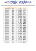
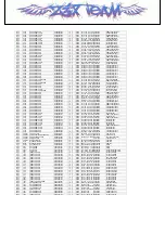
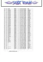
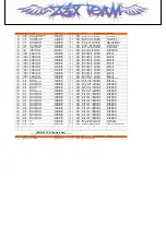

LGE
Doc.Name
SHEET OF
DRAW
DATE
CHKD
APRD
REF
MAN
ISSUE
CONTENT
LG<41>-A-2011.0
LGE Proprietary
Duplication of this document and the use or communication of the contents thereof are forbidden without express authority. Offenders are punishable and liable to the payment of damages.
All rights are reserved in the event of the grant of a patent or the registration of a utility model.
CELL_OUTP
KYPD[9]
+2.6V_TX
RCV/SPK_MODE
EAR_SPK
+VPWR
KYPD[13]
KYPD[15]
LNA_OUT
+2.6V_MSMP
KYPD[11]
TEMP_ADC
CELL_OUTM
MIC_BIAS
PA_ON
+2.85V_TCXO
+2.8V_BACK_END
UIM_CLK
KYPD_EN/
BATT_ADC
TX_CP
UIM_DATA
VIB_EN/
PA_R0
KYPD[17]
QSC_
+2.6V_RX
RX_CP
+2.65V_MSMA
+1.2V_MSMC
+2.85V_RUIM
RESIN/
UIM_RESET/
QSC_AMP_OUT-
EAR10P
EAR10N
JTAG_PSHOLD
JTAG_PSHOLD
+1.8V_MSM_E1
MLED_EN
FM_GPIO2
FM_I2C_SCL
FM_AMP_EN
FM_RESET/
EARSPK/FM_EARMOD
EBI1_OE/
EBI1_UB/
EBI1_LB/
EBI1_WE/
EAR_SENSE/
BACK_END_CLK/
LCD_RESET/
+3.0V_FM_EN
UART_TP_SEN
R202
10k
R225
470k
R219
5.76k
+/-1%
R226
470k
R235
4.7
R212
15k
+/-1%
R229
470k
+/-1%
R217
11.8k
+/-1%
R227
80.6k
+/-1%
R221
47k
R231
22
R214
12k
+/-1%
R220
10
R234
4.7
R222
10k
R232
5.6k
R233
5.6k
R239
5.6k
R228
121k
+/-1%
R241
33k
R242
33k
C272
100p
C250
100p
C261
470p
C217
3.3n
C251
100p
C252
1n
C255
100p
C205
8.2n
C244
100p
C220
1u
C268
220n
C202
220p
C226
100p
C242
100p
C210
1n
C222 0.1u
C223 0.1u
C224
0.1u
C225
0.1u
C229 0.1u
C233
0.1u
C237
0.1u
C241
0.1u
C227
0.1u
C231
0.1u
C238
0.1u
C247
0.1u
C253
0.1u
C257
0.1u
C239
0.1u
C246
0.1u
C230
0.1u
C235
0.1u
C245
0.1u
C254
0.1u
C258
0.1u
C232
0.1u
C236
0.1u
C240
0.1u
C248
0.1u
C214
47n
C256
0.1u
C260
0.1u
C275
0.1u
C263
0.1u
C264
0.1u
C276
0.1u
C274
0.1u
C269 0.1u
C273
0.1u
C270
0.1u
C267
82n
C266
82n
C265
82n
C271
68n-16V
C262
68n-16V
+2.85V_TCXO
+2.85V_TCXO
RTCK
TMS
KEY_SENSE[1]
PWR_ON_SW/
TDO
RESIN/
+2.6V_RX
+VPWR
KEY_SENSE[3]
MIX_INP
TDI
+2.6V_MSMP
TEMP_ADC
+2.6V_MSMP
TCK
MIC+
MIX_INM
KEY_SENSE[4]
+VPWR
RX_CP
TDI
+1.2V_MSMC
KEY_SENSE[0]
+2.6V_MSMP
KEY_SENSE[2]
USB_D+
RTCK
TDO
V_CHAR
TMS
+VPWR
+2.6V_TX
LNA_IN
EAR_MIC
+2.6V_MSMP
EARPHONE_KEY
TCK
BATT_ADC
TX_CP
+2.65V_MSMA
+VPWR
V_CHAR
PWR_ON_SW/
TRST_N
TRST_N
BATT_DET_ADC
FM_I2C_SDA
+1.8V_MSM_E1
FM_AFR
USB_D-
USB_POWER
USB_D-
USB_D+
MSM_DP_RXD
MSM_DP_TXD
MSM_DP_RXD
MSM_DP_TXD
DC_PWR_SEN/
IO_DET_ADC
USB_POWER
UART_TP_SEN
R218
DNI
1005
R223
DNI
1005
R224
DNI
1005
R240
DNI
2SB1424
Q201
1
B
3
E
2
C
C216
2.2u-6.3V
1608
C218
2.2u-6.3V
1608
C207
2.2u-6.3V
1608
C209
2.2u-6.3V
1608
C243
2.2u-6.3V
1608
C228
2.2u-6.3V
1608
C219
2.2u-6.3V
1608
C234
2.2u-6.3V
1608
C249
4.7u
1608
C212
2.2u-6.3V
1608
C213
2.2u-6.3V
1608
C201
1u-10V
1608
R230
1608
NCP18WM154J03RB
1
2
R213
0.1
2012R
+/-1%
UART-TP
U202
1
GND
2
UART-RXD
3
UART-TXD
4
V_CHAR
5
ON_SW
6
VBATT
7
USB-POWER
8
USB-RXD
9
USB-TXD
10
CHAR_MON
11
KEY_LED_EN
12
NC1
JTAG_STANDARD_10PIN
CON201
1
2
3
4
5
6
7
8
9
10
MIP2520D4R7M
L203
1
2
C215
DNI
1005
C204
DNI
1005
C259
DNI
1005
L201
22n
L202
22n
QSC6010
U201
Y1
PA_ON
AA3
PA_R0
L22
CELL_OUTM
M22
CELL_OUTP
J22
TX_CP
K16
RBIAS_TX
A18
LNA_IN
B21
LNA_OUT
D22
MIX_INM
E22
MIX_INP
G22
RX_CP
B20
RBIAS_LNA
R13
TRK_LO_ADJ
T15
XO_TUNE
R14
TCXO_OUT
AB19
XTAL_19M_IN
AB20
XTAL_19M_OUT
W22
XTAL_32K_IN
Y22
XTAL_32K_OUT
B12
HKAIN0
D12
HKAIN1
R21
MPP1
R22
MPP2
M15
CBL_PWR_N
N16
KPD_PWR_N
R15
PS_HOLD
P15
KPD_DRV_N
P16
VIB_DRV_N
R16
LCD_DRV_N
N15
VDD_IN1
P18
VDD_IN2
T19
VDD_IN3
U19
VDD_IN4
V14
VDD_IN5
W14
VDD_IN6
W21
VDD_IN7
AA18
VDD_IN8
AB14
VDD_IN_CORE
W15
VCOIN
V15
VCHG
W16
CHG_CNT_N
AA15
ISNS_P
AA16
ISNS_M
W17
BAT_FET_N
V16
VBAT
T21
VREG_RFRX
T22
VREG_RFTX
AA14
VSW_MSMC
AB15
VREG_MSMC
W13
VREG_MSMC_S
V21
VREG_MSME1
V22
VREG_MSME2
P19
VREG_MSMP
AB12
VREG_MSMA
AA13
VREG_RUM
N11
VREG_TXCO
AB18
VREG_USB
A20
VDD_RFRX1
C21
VDD_RFRX2_1
D21
VDD_RFRX2_2
E21
VDD_RFRX2_3
F22
VDD_RFRX3_1
G21
VDD_RFRX3_2
H18
VDD_RFRX4
H22
VDD_RFTX1_1
J21
VDD_RFTX1_2
K21
VDD_RFTX1_3
K22
VDD_RFTX2
N22
VDD_RFTX3
N19
VDD_RFTX5
N21
VDD_RFTX4_1
P21
VDD_RFTX4_2
P22
VDD_RFTX4_3
B5
VDD_CORE1
B11
VDD_CORE2
J2
VDD_CORE3
T12
VDD_CORE4
U2
VDD_CORE5
AA6
VDD_CORE6
AA8
VDD_CORE7
B4
VDD_P1_1
B7
VDD_P1_2
B9
VDD_P1_3
G2
VDD_P2_1
L2
VDD_P2_2
B10
VDD_P3_1
P2
VDD_P3_2
V2
VDD_P3_3
V13
VDD_P3_4
M4
UART1_RFR_N/GPIO(56)
N8
UART1_CTS_N/GPIO(55)
U4
GPIO(54)
Y2
CAM_DATA_7/GPIO(53)
V5
CAM_DATA_6/GPIO(52)
V7
CAM_DATA_5/GPIO(51)
U5
CAM_DATA_4/GPIO(50)
W4
CAM_DATA_3/GPIO(49)
W8
CAM_DATA_2/GPIO(48)
W5
CAM_DATA_1/GPIO(47)
V6
CAM_DATA_0/GPIO(46)
W6
GPIO(45)
V8
CAM_PCLK/GPIO(42)
W7
CAM_HSYNC/GPIO(43)
T7
CAM_VSYNC/GPIO(44)
W2
GPIO(35)
AB3
CAM_FLASH/GPIO(33)
AB11
GPIO(32)
V4
GP_MN/GPIO(30)
N5
RINGER/GPIO(29)
B2
GPIO(28)
C2
GPIO(27)
D2
GPIO(23)
M5
GPIO(24)
N4
GP_PDM_2/GPIO(21)
P8
UART2_RX_D/GPIO(20)
P7
I2C_SCL/GPIO(19)
T2
I2C_SDA/GPIO(18)
E2
GPIO(14)
R1
GPIO(13)
AA11
UART2_TX_D/UIM_DATA/GPIO(11)
AA12
UART2_RFR_N/UIM_CLK/GPIO(10)
V12
UART2_CTS_N/UIM_RESET/GPIO(9)
N7
BACKLIGHT_EN/GP_PDM_0/GPIO(8)
R2
HEADSET_DET_N/GPIO(7)
T1
PCM_CLK/SDAC_CLK/GPIO(6)
T8
PCM_DOUT/SDAC_DOUT/GPIO(5)
R9
PCM_DIN/SDAC_MCLK/GPIO(4)
AB7
PCM_SYNC/SDAC_L_R/GPIO(3)
AA4
UART1_RX_D
AB4
UART1_TX_D
W18
USB_ID
AB16
USB_DP
AB17
USB_DM
AA17
USB_VBUS
AA7
KYPD_17/GPIO(1)
T9
KYPD_15/GPIO(2)
AA2
KYPD_13/MSM_DP_DTR/GPIO(36)
R7
KYPD_11/GPIO(0)
P4
KYPD_9/GP_PDM_1/GPIO(12)
T4
KEYSENSE_4N/GPIO(38)
R4
KEYSENSE_3N/GPIO(39)
T5
KEYSENSE_2N/GPIO(40)
R5
KEYSENSE_1N/GPIO(41)
W1
KEYSENSE_0N/GPIO(37)
R8
KYPD_MEMO/GPIO(17)
D15
MIC1N
D16
MIC1P
B16
MIC2N
B17
MIC2P
A17
MIC_BIAS
D13
HPH_OUT
A15
EAR1OP
A16
EAR1ON
B14
AUXOP
B15
AUXON
U21
SPKR_IN_P
U22
SPKR_IN_M
V19
SPKR_OUT_P
W19
SPKR_OUT_M
E14
CCOMP
AA21
REF_ISET
AA20
REF_BYP
AA19
REF_GND
V18
GND_P_SPKR1
Y21
GND_P_SPKR2
T18
GND_P_RF1
R19
GND_P_RF2
U18
GND_P_DRVR1
N18
GND_P_DRVR2
AB13
GND_MSMC
V17
GND_P_GEN1
T16
GND_P_GEN2
R18
GND_P_GEN3
N13
GND_TCXO
M12
GND_B_SR9
M11
GND_B_SR8
L12
GND_B_SR7
L11
GND_B_SR6
H11
EBI_A_24
G10
EBI_A_23
E8
EBI_A_22
D9
EBI_A_21
H10
EBI_A_20
A8
EBI_A_19
E9
EBI_A_18
B8
EBI_A_17
G9
EBI_A_16
E4
EBI_A_15
D4
EBI_A_14
D5
EBI_A_13
E5
EBI_A_12
F5
EBI_A_11
D6
EBI_A_10
G7
EBI_A_9
D7
EBI_A_8
H8
EBI_A_7
B6
EBI_A_6
E6
EBI_A_5
A6
EBI_A_4
G8
EBI_A_3
D8
EBI_A_2
H9
EBI_A_1
E7
EBI_A_0
F4
EBI_D_15
H4
EBI_D_14
H5
EBI_D_13
H7
EBI_D_12
J4
EBI_D_11
H2
EBI_D_10
J5
EBI_D_9
H1
EBI_D_8
J7
EBI_D_7
K4
EBI_D_6
K2
EBI_D_5
J8
EBI_D_4
K5
EBI_D_3
K7
EBI_D_2
K8
EBI_D_1
L4
EBI_D_0
L7
EBI_RESOUT_N
N2
GPIO(15)/EBI_MEM_CLK
G4
EBI_WE_N
G5
EBI_OE_N
F2
EBI_LB_N
E1
EBI_UB_N
D1
GPIO(22)/EBI_CS7_N
A10
EBI_CS6_N
C1
GPIO(26)/EBI_CS5_N
D10
EBI_CS4_N
M8
GPIO(31)/EBI_CS3_N
M2
EBI_CS2_N
N1
GPIO(25)/EBI_CS1_N
M1
EBI_CS0_N
F1
EBI_BSY_N
B3
EBI_WAIT_N
A3
EBI_ADV_N
L1
LCD_CS_N
L8
LCD_EN
L5
LCD_RS
A1
NC1
A2
NC2
B1
NC3
AA1
NC4
AB1
NC5
AB2
NC6
AA22
NC7
AB21
NC8
AB22
NC9
A22
NC10
B22
NC11
C22
NC12
A19
DNC1
A21
DNC2
B18
DNC3
B19
DNC4
K13
DNC5
L13
DNC6
M13
DNC7
N10
DNC8
N12
DNC9
E10
DNC10
G11
DNC11
AA5
VDD_P3_5
AA10
VDD_P3_6
B13
VDD_A_AN1
E12
VDD_A_AN2
E13
VDD_A_AN3
E15
VDD_A_AN4
G13
VDD_A_AN5
G14
VDD_A_AN6
H12
VDD_B_AN1
L10
VDD_B_AN2
V9
TRST_N
T10
TCK
AB9
TMS
T11
TDI
R10
TDO
W9
RTCK
T14
PON_RESET_N
T13
RESIN_N
AA9
RESOUT_N
W10
RSRVD
V11
WDOG_EN
W11
MODE_1
V10
MODE_0
W12
EBI_MODE
P5
TRUSTED_BOOT/GPIO(16)
M7
FAILED_TB/GPIO(34)
A13
GND_A_AN1
A14
GND_A_AN2
D11
GND_A_AN3
D14
GND_A_AN4
E11
GND_A_AN5
E16
GND_A_AN6
H13
GND_A_AN7
H14
GND_A_AN8
H15
GND_A_AN9
G15
GND_A_GR1
L15
GND_A_GR2
K18
GND_A_RF1_1
K19
GND_A_RF1_2
L16
GND_A_RF1_3
L18
GND_A_RF1_4
L19
GND_A_RF1_5
L21
GND_A_RF1_6
M16
GND_A_RF1_7
M18
GND_A_RF1_8
M19
GND_A_RF1_9
M21
GND_A_RF1_10
G18
GND_A_RF2_1
G19
GND_A_RF2_2
H19
GND_A_RF2_3
H21
GND_A_RF2_4
J18
GND_A_RF2_5
J19
GND_A_RF2_6
F18
GND_A_RF3_1
F19
GND_A_RF3_2
F21
GND_A_RF3_3
D17
GND_A_RF4_1
D18
GND_A_RF4_2
D19
GND_A_RF4_3
E17
GND_A_RF4_4
E18
GND_A_RF4_5
E19
GND_A_RF4_6
G12
GND_B_AN1
K11
GND_B_AN2
K12
GND_B_AN3
A5
GND_B_CORE1
A11
GND_B_CORE2
J1
GND_B_CORE3
R12
GND_B_CORE4
U1
GND_B_CORE5
AB6
GND_B_CORE6
AB8
GND_B_CORE7
A4
GND_B_DIG1
A7
GND_B_DIG2
A9
GND_B_DIG3
A12
GND_B_DIG4
G1
GND_B_DIG5
K1
GND_B_DIG6
M10
GND_B_DIG7
P1
GND_B_DIG8
R11
GND_B_DIG9
V1
GND_B_DIG10
AB5
GND_B_DIG11
AB10
GND_B_DIG12
G16
GND_B_SR1
H16
GND_B_SR2
J15
GND_B_SR3
J16
GND_B_SR4
K15
GND_B_SR5
10u-10V
C206
R203
0
R204
0
R209
0
R205
0
R206
0
R207
0
R215
0
R216
0
R237
DNI
R238
0
C211
4.7u
2012
TP212
DSX321G_19_2MHZ_8PF
X201
1
2
3
4
C278
100n
R243
1k
Rev1.0
2 5
2007.12.07
Condition
19.2 M Crystal Change
225 ~500mA ->
<TEMP. CHECK>
Current is not used ->
TYPE
Range
150mA ->
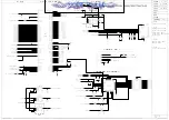
Buck / 500mA ON / 1.3V 0.75 ~ 3.05V - Core
MSMP / 300mA ON / 2.6V 1.5 ~ 3.05V - PAD FOR I/O
MSMA / 150mA ON / 2.6V 1.5 ~ 3.05V - Analog
MSME1 / 150mA ON / 1.8V 1.5 ~ 3.05V - EBI1 Circuits
MSME2 / 150mA ON / 2.9V 1.5 ~ 3.05V - EBI2 Circuits
RFRX / 150mA OFF/ 2.6V 1.5 ~ 3.05V - RF RX
RFTX / 150mA OFF/ 2.6V 1.5 ~ 3.05V - RF TX
RUIM / 150mA OFF/ 2.85V 1.5 ~ 3.05V - RUIM
(1.8V & 3.0V Support)
TCXO / 50mA ON / 2.85V 1.5 ~ 3.05V - XO
USB / 50mA OFF/3.3V 3.0V ~ 6.1V - USB Circuit--
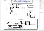
< JTAG POINT >
<Battery Level>
R237, R238 Inserted:
EBI Dual mode control
QSC6030_MEMORY
QSC6030_MEMORY
<TP ARRAY>
QSC6030
Dual EBI mode
<PCB REVISION>
PCB REVISON LOGIC
PCB Version GPIO Change
BATT_DET ADC Change
<PCB_REV 3>
<PCB_REV 1>
<PCB_REV 2>
<RevB>
<RevC>
Delete:C221,R236(3.0V VTRM)
Insert:TP211
TP210, TP211,R204
<RevD>
Insert:GPIO56
<Rev1.0>
Change:X201
Insert:R243,C278
1.1 H L H
Revison REV 1 REV 2 REV 3
1.3 H H H
1.0 H L L
C L L L
1.2 H H L
F L H H
D L L H
E L H L
Z3X-BOX.COM
Summary of Contents for LG-UD6100
Page 25: ...Circuit Diagram Z 3 X B O X C O M ...
Page 40: ...Test Points Circuit Diagram 4 3 5 UIM Trouble CON301 3 0V 3 2 1 Z 3 X B O X C O M ...
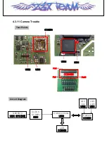
Page 46: ...Test points Circuit Diagram 4 3 8 MIC Trouble R371 C327 M301 MIC Z 3 X B O X C O M ...
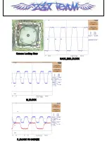
Page 55: ...BACK_END_CLOCK M_CLOCK P_CLOCK VS DATA 0 Camera Locking Error Z 3 X B O X C O M ...
Page 62: ...Z 3 X B O X C O M 0 Ohm Pad 0 Ohm Pad DNI DNI ...
Page 63: ...Z 3 X B O X C O M 0 Ohm Pad 0 Ohm Pad DNI DNI ...
Page 64: ...Z 3 X B O X C O M ...
Page 65: ...Z 3 X B O X C O M ...
Page 66: ...Z 3 X B O X C O M ...


