- 4-18 -
DECK MECHANISM ADJUSTMENT
Purpose: To correct for shift in the Roller Guide and X value after replacing the Drum.
8-2. Checking for tape curling or jamming
Test Equipment/ Fixture
T-160 Tape
T-120 Tape
Specification
Be sure there is no tape jamming or curling at
the begining, middle or end of the tape.
VCR(VCP) State
Run the CUE, REV, Play mode at the
beginning and the end of the tape.
Test Conditions (Mechanism Condition)
1) Confirm that the tape runs smoothly around the roller
guides, Drum and A/C Head Assemblies while abruptly
changing operating modes from Play to CUE or REV.
This is to be checked at the begining, middle and end
sections of the tape.
2) Confirm that the tape passes over the A/C Head
Assembly as indicated by proper audio reproduction and
proper tape counter performance.
Checking Procedure
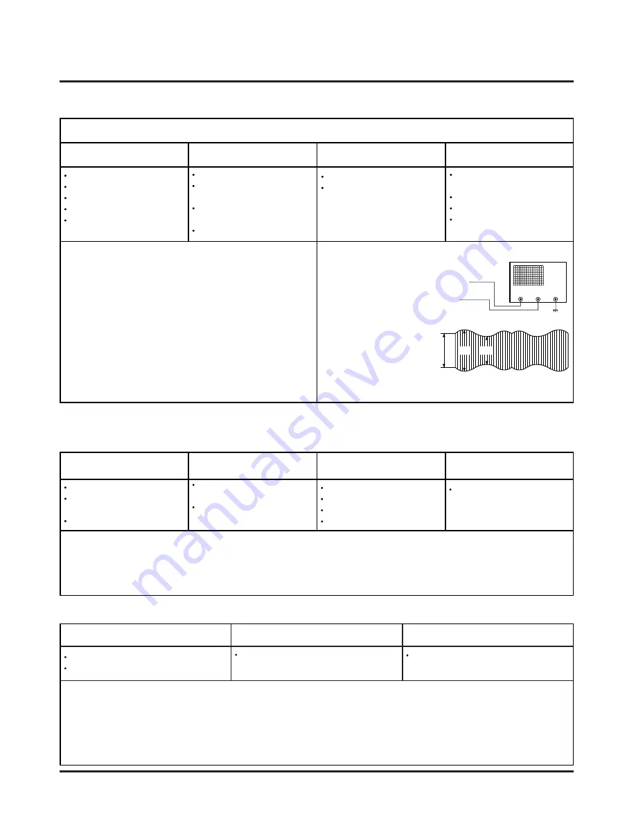
7. Adjustment after Replacing Drum Assembly (Video Heads)
Test Equipment/ Fixture
Oscilloscope
Alignment Tapes
Blank Tape
Post Height Adjusting Driver
Screw ) Type 5mm
Connection Point
CH-1: PB RF Envelope
CH-2: NTSC: SW 30Hz
PAL: SW 25Hz
Head Switching Output
Test Point
RF Envelope Output Test Point
Test Conditions
(Mechanism Condition)
Play the Blank Tape
Play an Alignment Tape
Adjustment Points
Guide Roller Precise
Adjustment
Switching Point
Tracking Preset
X-Value
Checking/Adjustment Procedure
Play a blank tape and check for tape curling or creasing around
the Roller Guide. If there is a problem then follow the procedure
4. "Guide Roller Height" and 5. "Audio Control(A/C) Head
Adjustment".
RF ENVELOPE OUTPUT TEST POINT
OSCILLOSCOPE
HEAD SWITCHING OUTPUT TEST
POINT
Connection Diagram
Waveform
V1/V MAX
E
0.7
V2/V MAX
E
0.8
RF ENVELOPE OUTPUT
Fig. C-7
8. Check the Tape Travel after Reassembling Deck Assembly.
8-1. Checking Audio and RF Locking Time during playback and after CUE or REV (FF/REW)
Test Equipment/ Fixture
Oscilloscope
Alignment Tapes(with 6H
3KHz Color Bar Signal)
Stop Watch
Specification
RF Locking Time: Less than 5
sec.
Audio Locking Time:Less than
10sec
Test Equipment
Connection Points
CH-1: PB RF Envelope
CH-2: Audio Output
RF Envelope Output Point
Audio Output Jack
Test Conditions
(Mechanism Condition)
Play an Alignment Tape
(with 6H 3kHz Color Bar
Signal)
Checking Procedure
Play an Alignment Tape then change the operating mode to
CUE or REV and confirm if the unit meets the above listed
specifications.
NOTES:
1) CUE is the forward search mode
2) REV is the backward search mode
3) Refer to the Play mede
V1
V
V2
CH1 CH2
Connection Points
Summary of Contents for LH-C6230P
Page 10: ... 2 1 SECTION 2 AUDIO PART ...
Page 12: ... 3 2 VCR ELECTRICAL TROULBESHOOTING ...
Page 13: ... 3 3 ...
Page 27: ... 5 1 DVD ELECTRICAL TROUBLESHOOTING 1 Test debug flow SECTION 5 DVD PART ...
Page 28: ... 5 2 ...
Page 29: ... 5 3 ...
Page 30: ... 5 4 ...
Page 31: ... 5 5 ...
Page 32: ... 5 6 ...
Page 36: ... 5 10 2 Tray close waveform 3 Tray open waveform ...
Page 38: ... 5 12 6 LASER POWER CONTROL RELATED SIGNAL NO DISC CONDITION 7 DISC TYPE JUDGEMENT WAVEFORM ...
Page 39: ... 5 13 ...
Page 40: ... 5 14 8 FOCUS ON WAVEFORM ...
Page 41: ... 5 15 9 SPINDLE CONTROL WAVEFORM NO DISC CONDITION ...
Page 42: ... 5 16 10 TRACKING CONTROL RELATED SIGNAL System checking ...
Page 43: ... 5 17 11 RF WAVEFORM 12 MT1379 AUDIO OPTICAL AND COAXIAL OUTPUT ASPDIF ...
Page 44: ... 5 18 13 MT1379 VIDEO OUTPUT WAVEFORM 1 Full colorbar signal CVBS 2 Y ...
Page 45: ... 5 19 3 C 14 AUDIO OUTPUT FORM AUDIO DAC 1 Audio related Signal ...
Page 46: ... 5 20 MEMO ...
Page 49: ...2 2 2 3 BLOCK DIAGRAM ...
Page 50: ...2 4 2 5 AUDIO SHEMATIC DIAGRAMS U COM SCHEMATIC DIAGRAM ...
Page 51: ...2 6 2 7 FUNCTION POWER SCHEMATIC DIAGRAM ...
Page 52: ...2 8 2 9 MAIN AMP SCHEMATIC DIAGRAM ...
Page 53: ...2 10 2 11 WIRING DIAGRAM ...
Page 55: ...2 14 2 15 PRINTED CIRCUIT DIAGRAM MAINAMP FRONT P C BOARD SOLDER SIDE ...
Page 56: ...2 16 2 17 MAINAMP FRONT P C BOARD COMPONENT SIDE ...
Page 57: ...2 18 2 19 FUNCTION POWER P C BOARD SOLDER SIDE ...
Page 58: ...2 20 2 21 FUNCTION POWER P C BOARD COMPONENT SIDE ...
Page 59: ...3 17 3 18 VCR SHEMATIC DIAGRAMS SYSTEM SCHEMATIC DIAGRAM ...
Page 60: ...3 19 3 20 A AUDIO V VIDEO SCHEMATIC DIAGRAM ...
Page 62: ...3 23 3 24 TU IF ACSS SCHEMATIC DIAGRAM ...
Page 63: ...3 25 3 26 HIFI TUNER SCHEMATIC DIAGRAM ...
Page 64: ...3 27 3 28 A V JACK SCART SCHEMATIC DIAGRAM ...
Page 66: ...3 31 3 32 PRINTED CIRCUIT DIAGRAMS TUNER P C BOARD ...
Page 67: ...3 33 3 34 VCR P C BOARD ...
Page 68: ...3 35 3 36 VCR P C BOARD ...
Page 69: ...5 22 5 21 DVD PART SCHEMATIC DIAGRAMS MPEG SCHEMATIC DIAGRAM ...
Page 70: ...5 23 5 24 SERVO SCHEMATIC DIAGRAM ...
Page 71: ...5 25 5 26 AUDIO SCHEMATIC DIAGRAM ...
Page 72: ...5 27 5 28 INTERFACE SCHEMATIC DIAGRAM ...
Page 73: ...5 29 5 30 VOLTAGE SHEET IC TR ...
Page 74: ...5 31 5 32 PRINTED CIRCUIT DIAGRAM DVD P C BOARD SOLDER SIDE ...
Page 75: ...5 33 5 34 DVD P C BOARD COMPONENT SIDE ...
Page 77: ...SECTION 4 MECHANSIM OF VCR PART ...
Page 89: ... 4 12 ...
Page 101: ... 4 24 ...
Page 113: ......


