4-37
• Data is recorded by changing the recording layer from the amorphous status to the crystalline status, and played
back by reading the difference of the reflection coefficient.
Amorphous: Non-crystalline.
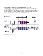
[ Recording ]
When a high-power laser is applied to the recording material, it melts and then becomes amorphous with a low
reflection coefficient when it quickly cools off. When a mid-power laser is applied to heat gradually the recording
material and then gradually cools it off, it becomes crystal with a high reflection coefficient.
[ Playback ]
A low-power laser is used for playback. The amount of reflected light depends on the status (amorphous or crys-
talline) of the recording material. This is detected by an optical sensor.
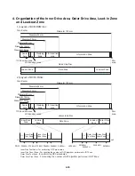
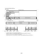
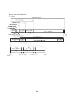
3) Recording format using phase-change recording material
( DVD-RW / DVD+RW )
G
Disc structure
G
Recording principles
Summary of Contents for LRM-519
Page 30: ...3 16 WAVEFORMS 1 SYSTEM PART 1 ...
Page 31: ...3 17 2 SYSTEM PART 2 ...
Page 32: ...3 18 3 VIDEO PART 1 ...
Page 33: ...3 19 4 VIDEO PART 2 ...
Page 34: ...3 20 5 VIDEO PART 3 ...
Page 35: ...3 21 6 VIDEO PART 4 ...
Page 36: ...3 22 AI_DATA AI_CLK AI_LRCLK 7 AUDIO PART 1 ...
Page 37: ...3 23 AUD_LINK_BCLK AUD_LINK_SDIN AUD_LINK_SYNC AUD_LINK_RST 8 AUDIO PART 2 ...
Page 38: ...SPDIF 3 24 AUDIO_L 9 AUDIO PART 3 ...
Page 39: ...3 25 TXD TXD RXIN RXIN 25MHZ 10 ETHERNET PART ...
Page 40: ...3 26 FLD_RXD FLD_CLK CLK_LPC_33MHZ 11 SUPER IO FRONT INTERFACE PART ...
Page 43: ...3 29 3 POWER BLOCK DIAGRAM ...
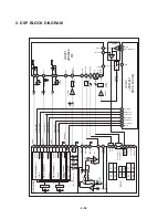
Page 45: ...3 31 5 BLOCK DIAGRAM ...
Page 46: ......
Page 48: ...3 34 3 35 2 POWER CIRCUIT DIAGRAM A B C D E F G H I J K L M N O P Q R S T ...
Page 49: ...3 36 3 37 3 CPU CIRCUIT DIAGRAM A B C D E F G H I J K L M N O P Q R S T ...
Page 50: ...3 38 3 39 4 GMCH CIRCUIT DIAGRAM A B C D E F G H I J K L M N O P Q R S T ...
Page 51: ...3 40 3 41 5 ICH4 CIRCUIT DIAGRAM A B C D E F G H I J K L M N O P Q R S T ...
Page 52: ...3 42 3 43 6 CLOCK LPC CIRCUIT DIAGRAM A B C D E F G H I J K L M N O P Q R S T ...
Page 53: ...3 44 3 45 7 MEMORY IDE CIRCUIT DIAGRAM A B C D E F G H I J K L M N O P Q R S T ...
Page 54: ...8 LAN USB MODEM CIRCUIT DIAGRAM A B C D E F G H I J K L M N O P Q R S T 3 46 3 47 ...
Page 57: ...3 52 3 53 11 TUNER EXTERNAL AV INPUT CIRCUIT DIAGRAM A B C D E F G H I J K L M N O P Q R S T ...
Page 59: ...3 56 3 57 13 MISCELLANEDUS CIRCUIT DIAGRAM A B C D E F G H I J K L M N O P Q R S T ...
Page 60: ...3 58 3 59 14 EXTERNAL I F CIRCUIT DIAGRAM A B C D E F G H I J K L M N O P Q R S T ...
Page 61: ...3 60 3 61 PRINTED CIRCUIT DIAGRAMS 1 MAIN PRINTED CIRCUIT DIAGRAMS TOP VIEW ...
Page 62: ...3 62 3 63 2 MAIN PRINTED CIRCUIT DIAGRAMS BOTTOM VIEW ...
Page 64: ...3 66 3 67 5 POWER PRINTED CIRCUIT DIAGRAM ...
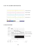
Page 84: ...4 20 9 LASER TURN ON SIGNAL F LIC502 PIN 52 LDEN DVD LCN201 PIN17 VRDC LCN201PIN 34 ...
Page 99: ...4 35 2 Disc Specification 3 Disc Materials 1 DVD ROM Single Layer Dual Layer ...
Page 119: ...4 55 4 56 CIRCUIT DIAGRAMS 1 RF CIRCUIT DIAGRAM A B C D E F G H I J K L M N O P Q R S T ...
Page 120: ...4 57 4 58 2 DSP CIRCUIT DIAGRAM A B C D E F G H I J K L M N O P Q R S T ...
Page 121: ...4 59 4 60 3 µ COM CIRCUIT DIAGRAM A B C D E F G H I J K L M N O P Q R S T ...
Page 123: ...4 63 4 64 PRINTED CIRCUIT DIAGRAMS 1 MAIN P C BOARD LOCATION GUIDE ...


