3-36
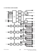
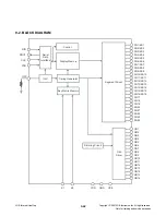
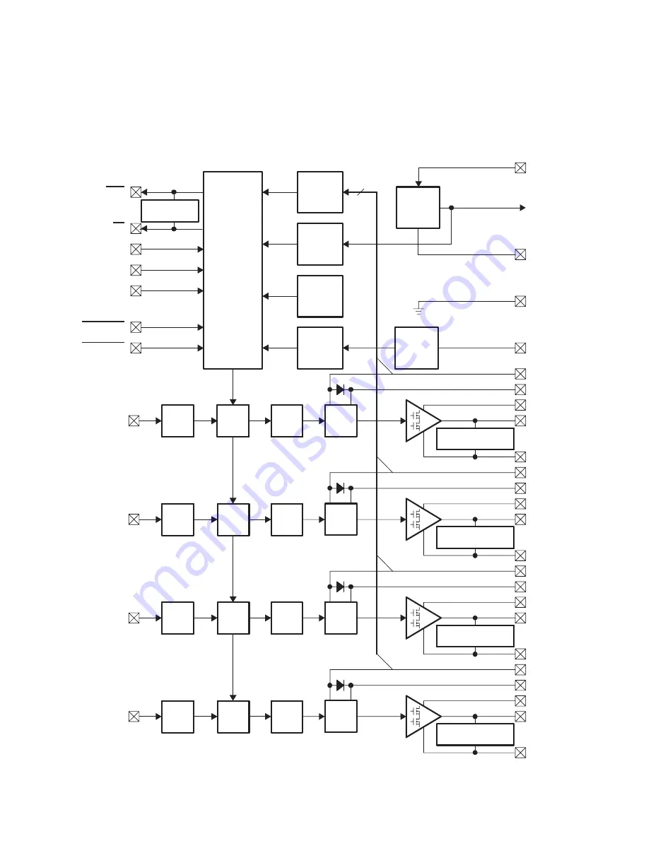
4-3. FUNCTIONAL BLOCK DIAGRAM
Temp.
Sense
M1
M2
RESET_AB
SD
OTW
AGND
OC_ADJ
VREG
VREG
VDD
M3
Power
On
Reset
Under-
voltage
Protection
GND
PWM_D
OUT_D
GND_D
PVDD_D
BST_D
Timing
Gate
Drive
PWM
Rcv.
Overload
Protection
Isense
GVDD_D
RESET_CD
4
Protection
and
I/O Logic
PWM_C
OUT_C
GND_C
PVDD_C
BST_C
Timing
Gate
Drive
Ctrl.
PWM
Rcv.
GVDD_C
PWM_B
OUT_B
GND_B
PVDD_B
BST_B
Timing
Gate
Drive
Ctrl.
PWM
Rcv.
GVDD_B
PWM_A
OUT_A
GND_A
PVDD_A
BST_A
Timing
Gate
Drive
Ctrl.
PWM
Rcv.
GVDD_A
Ctrl.
BTL/PBTL Configuration
Pulldown Resistor
BTL/PBTL Configuration
Pulldown Resistor
BTL/PBTL Configuration
Pulldown Resistor
BTL/PBTL Configuration
Pulldown Resistor
Internal Pullup
Resistors to VREG
Copyright © 2007 LG Electronics. Inc. All right reserved.
Only for training and service purposes
LGE Internal Use Only


