background image

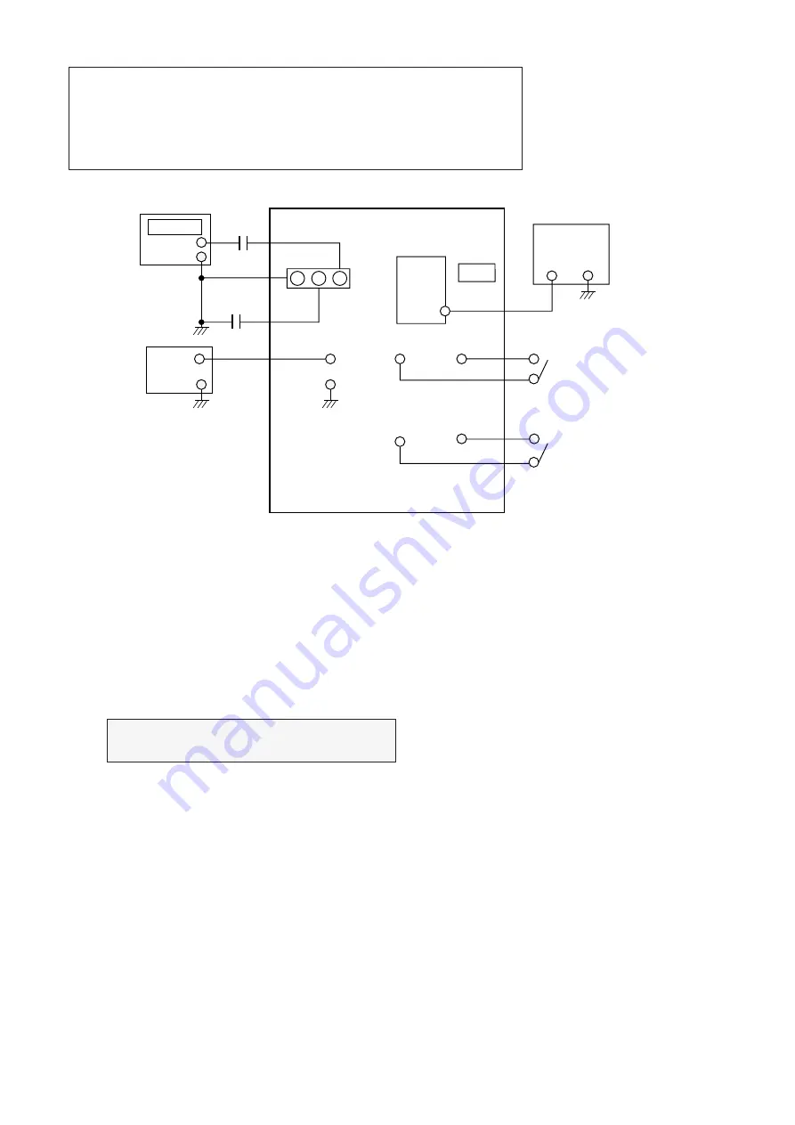
*  VCO (Voltage Controlled Oscillation) Adjustment

a) For B/G system

1)  Turn on DC power supplies.

2) Adjust VCO adjust coil(

L107

)so that DMM reads 2.5Vdc+_0.1V.

Preparation for VCO Adjustment

1.  Connect the measuring equipment to the TV as shown in Fig. 1.
2.  Set RF output level of sweep S.G.(Signal Generator) to 80dBuV.
3.  Set Alignment Scope, Volts/Div to 100mV, AC/DC switch to

AC, Line/Ext switch to Ext.

IC101
TDA4474

C123(+)

Multimeter &
oscilloscope
2.5Vdc

SW1

SW2

24

3

4

5

L107

J169  5V

GND

AM/FM SW

L/L'SW

Z101
G3962

J77

12Vdc

R124

C25(+)

R139

C25(-)

Power
Supply

GND(C26(-))

38.9MHz

Signal
generator

GND

Ceramic
CAP.
10000pF

Ceramic
CAP.
10000pF

MAIN BOARD

Fig.1: Connection Diagram of Equipment for BG VCO Adjustment

Test Poin t  : 

Pin 24 of IC101 (+ lead of C123)

Adjust  : 

L107

Summary of Contents for PC-63A

Page 1: ...HARGE from the electromaniacs com community You are free to distribute this file to other persons who needs it but without of charge Also on http electromaniacs com you can find thousands of service manuals schematics free of charge ...

Page 2: ...sweep S G Signal Generator to 80dBuV 3 Set Alignment Scope Volts Div to 100mV AC DC switch to AC Line Ext switch to Ext IC101 TDA4474 C123 Multimeter oscilloscope 2 5Vdc SW1 SW2 24 3 4 5 L107 J169 5V GND AM FM SW L L SW Z101 G3962 J77 12Vdc R124 C25 R139 C25 Power Supply GND C26 38 9MHz Signal generator GND Ceramic CAP 10000pF Ceramic CAP 10000pF MAIN BOARD Fig 1 Connection Diagram of Equipment fo...

Page 3: ...creen VR of FBT until the black level of picutre signal is 150Vdc at the digital pattern IC101 TDA4474 C123 GND C122 Multimeter oscilloscope 2 5Vdc SW1 SW2 24 3 4 5 VR102 J139 GND 5V AM FM SW L L SW Z102 G3953 J77 12Vdc R124 C25 R169 C25 Power Supply GND C26 33 9MHz Signal generator GND Ceramic CAP 10000pF Ceramic CAP 10000pF MAIN BOARD Fig 2 Connecting Diagram of Equipments for secam L system Tes...

Page 4: ...he RF signal is at least 1mV 60dBu the picture will be noise free in any area Adjusting th e VR101 RF AGC control to one end of rotation will usually cause a relatively poor signal to noise ratio Adjusting to the other end of rotation will usually cause a degradation of over load capabilities resulting in color beats or adjacent channel reference For best results adjust VR101 control while perform...

Page 5: ...mpletely forward 5 Reconnect the internal degaussing coil 6 Position the beam bender locking rings at the 9 o clock position and the other three pairs of tabs 2 4 and 6 pole magnets at the 12 o clock position 7 Perform the following steps in the order given to prepare the receiver for the purity adjustment procedure a Face the receiver in the magnetic north direction b Externally degauss the recei...

Page 6: ...nal degaussing coil 9 Turn on the receiver connect a signal generator to the VHF antenna terminal and apply a crosshatch signal Caution During the convergence adjustment procedure be very careful not to disturb the purity adjustment tabs are accidentally move purity should be confirmed before proceeding with the convergence adjustments Note Make sure the focus is set correctly on this instrument b...

Page 7: ... and blue horizontal lines Fig upper right 17 Temporarily place a rubber wedge at the 5 o clock and 7 o clock positions to hold the horizontal position of the yoke 18 Check the 3 o clock and 9 o clock areas to confirm that the red and blue vertical lines are converged If the lines are not converged slightly offset the horizontal tilt of the yoke move the temporary rubber wedges if necessary to equ...

Page 8: ...SSOR TDA 4780 VIDEO AMP SVM TDA6111Q X3 COLOR SW GD4052B H P AMP TDA2882 SOUND PROCESSOR MSP3410P LPF GL4558 L S AMP LA4282 IIC1 IIC1 AGC CVBS IF2 SW 2 2 2 Headphone SPEAKER1 L SPEAKER2 R 2 2 2 2 2 2 2 2 2 2 4 RGB FB CVBS RESET IIC0 IIC1 Addr Data Addr Data Co L R Y C L R V Lo Ro2 Li Ri2 Vo2 Vi2 Yi Ci Lo Ro1 Li Ri1 Vi1 Vo1 RGB FB 4 RGB FB IIC1 IIC1 H V YUV50 YUV100 RGB CPT A66EAK552X54 RGB IIC0 II...

Page 9: ...0 of IC702 Check the CVBS line Check Replace IC702 703 X701 Check I2 C BUS lines SDA SCL Check pin 51 52 53 and 54 of IC702 Check the voltage of CPT Heater Check the voltage of HV and SCREEN of CPT Check Replace CPT Board Check the Heater pulse at pin 9 of T701 Check Replace T701 Check Replace T701 Check Replace Connector FR459 and FR901 Check Replace IC503 ...

Page 10: ... Is the R Y B Y signal at pin 3 4 of IC501 normal Check Replace IC501 502 Is the Y U V in 50Hz signal at pin 12 13 and 14 of IC501 normal Check Replace IC101 Is the Y U V out 100Hz signal at pin 3 4 and 6 of P101 normal GO to DIGITAL BLOCK Is the R G B signal at pin 1 3 and 5 of IC501 normal Check Replace IC503 Check Replace IC503 NG NG NG NG NG NG ...

Page 11: ...SIF signal at pin26 of IC101 normal Check Replace IC101 Are the Audio signal at pin28 and 29 IC601 normal Are the Audio signal at pin 2 and 5 of IC605 normal Are the Audio signal at pin 7 and 11 of IC605 normal Check Replace Connectors and Speakers Check Replace X601 IC601 and IC606 Check LO RO lines Check Replace IC605 Sound B Line Check AM line NG NG NG NG NG NG ...

Page 12: ...rmal Is the CVBS signal at pin14 of IC101 normal yes yes OK OK no no no Go to NO PICTURE Block NO SOUND Block Check the voltages 5V 12V and 33V of Tuner Check Replace ZD101 102 5V 12V and 33V Lines Check Replace IC101 Check I2 C bus lines SDA SCL Check Replace TUNER ...

Page 13: ...or of Q402 normal Check Replace T701 and CONNECTORS Is the voltage at pin 24 of IC01 5V Check Replace IC803 D826 827 828 829 T805 T801 804 and Fuse FC02 Check the part of Digital PCB ASSY Check the voltage of C834 Check the voltage at pin9 of IC801 Check Replace D802 D803 Q801 and IC801 Check Replace D801 no Check Replace Q401 T401and Q402 Check Replace IC802 IC804 D810 and R832 ...

Page 14: ...101 Check Y U V signals at CQ54 CQ57 and CQ58 Check the Vcc of each IC Check Pin 34 40 and Pin 48 51 of ICQ05 Check Pin10 of ICQ06 Check Pin15 and 16 of ICQ06 for 27MHz and 13 5MHz waveform Check the Video Sync at CQ54 Check if Pin13 and 20 of ICQ01 have 32 s Check Pin61 68 and Pin2 5 of ICQ04 Check Pin13 16 Pin18 21 Pin22 25 of ICQ02 Check the outputs of Pin 2 4 5 of PQ102 no no no no no good no ...

Page 15: ......

Page 16: ......

Reviews: