background image

DLP PROJECTOR 

SERVICE MANUAL 

MODEL RD-JT50/51/52

CAUTION

BEFORE SERVICING THE PROJECTOR, 

READ THE SAFETY PRECAUTIONS IN THIS MANUAL. 

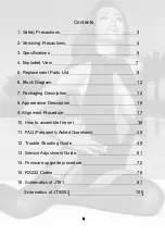
Summary of Contents for RD-JT51

Page 1: ...DLP PROJECTOR SERVICE MANUAL MODEL RD JT50 51 52 CAUTION BEFORE SERVICING THE PROJECTOR READ THE SAFETY PRECAUTIONS IN THIS MANUAL ...

Page 2: ... Block Diagram 12 7 Packaging Description 14 8 Appearance Description 16 9 Alignment Procedure 17 10 How to assemble the set 38 11 FAQ Frequently Asked Questions 48 12 Trouble Shooting Guide 49 13 Service Adjustment Guide 61 14 Firmware upgrade procedure 72 15 RS232 Codes 76 16 Schematics of JT51 81 Schematics of JT50 52 108 ...

Page 3: ...ò Ý º Èó º ª ò øÈó þ þ þ ó òþ Î ª ô º ô Èó º ª Ð Í º ú Èó É ª ò Ø ª º ó º ó ñ óª ò º ª º ô µ º µ ª ò îò Î º ó ª ô ª ô ò íò Ü ß É ó Ü º ÌÊ ª ò Ü ô ô ô º º ñ ª ô º º ª ò ß ª º ù µ ô ª º º ò ìò Ð Ì Ð É óÌ ª ò Ú ô º ò Ü ª ô ô º º ò Ð µ º ò Õ º ò Ü µò Í þ ó þ º µ å º ô ª þ þ µ º ò ëò Ø Ý É ó ò Í ÌÊ ª º ßÝ º ª º º ßÝ º ßÝ ò Ì º ßÝ ô ßÝ ª µ ò º ª º ïòð Ê ô ª ßÝ ª µ ò ò Í ÌÊ ª ª èë Ê ßÝ øÎÓÍ º ßÝ ò Ì º ª ...

Page 4: ... ò ìò ß ª º º ò Ì ª ò ò ëò ߺ ª ô µ ª ô ô ª ª ª ò Ú ô µ º ª ò ÒÍËÔßÌ ÑÒ ÝØÛÝÕ ÒÙ ÐÎÑÝÛÜËÎÛ Ü º ßÝ ò Ý øëðð Ê º ò Ì º ª øÒ ï ï Ó ò Ò æ ß ª ô ô µ ô ò ÛÔÛÝÌÎÑÍÌ ßÌ ÝßÔÔÇ ÍÛÒÍ Ì ÊÛ øÛÍ ÜÛÊ ÝÛÍ Í ø ó ª ò Í Û Í ª øÛÍ Ü ª ò Û º ÛÍ ª º ó ºº þ þ ò Ì º º ò ïò º ó ô ºº µ ò ß ª ô ª ª ô ª º µ ò îò ߺ ª ÛÍ ª ô ª º º ô ª º ò íò Ë ó ÛÍ ª ò ìò Ë ó ª ª ò Í ª ª º þ ó þ ºº ÛÍ ª ò ëò Ü º ó ò Ì ºº ÛÍ ª ò êò Ü ª ÛÍ ª º ...

Page 5: ...HIP DMD Lens F Number F 2 6 Lamp 200W NSH LAMP Electrical Power supply AC100 240V 3 2A 50 60 Hz Automatic Power consumption 285W Max Mechanical Dimensions 302 3mm W 91 7mm H 216 3mm D Operating temperature range 0 C 40 C Weight 6 6 lbs 3 0 Kg Input terminal Computer input D SUB IN D sub 15 pin female Video signal input S VIDEO Mini DIN 4 pin port x1 VIDEO RCA jack x1 HDTV signal input Dósub YpbPr ...

Page 6: ...240V 4 0A 50 60 Hz Automatic Power consumption 330W Typical Mechanical Dimensions 302 3mm W 91 7mm H 216 3mm D Operating temperature range 0 C 35 C Weight 6 6 lbs 3 0 Kg Input terminal Computer input D SUB IN D sub 15 pin female DVI D DVI D 19 pin female Video signal input S VIDEO Mini DIN 4 pin port x1 VIDEO RCA jack x1 HDTV signal input D sub YpbPr RCA jack x3 through D SUB IN Terminal Audio sig...

Page 7: ... 4 Exploded View The illustration shows exploded view of JT 51 projector You can see the major components and optical engine Main Board Lens Balleat Fan Board Lamp Box Rear Fan Module Chip Board AC cable ...

Page 8: ...AMP BOX PB6100 14 55 J1313 001 6871VSN257G PCB 1L SENSOR B BD SL700 X MI 15 65 J8603 001 3680V00118D CW DIA44DEG110 PB6100 PRODISC 16 23 10102 002 5900V03002J BLOWER 12V 50 50 20MM ADDA 17 60 J8640 001 3680V00075D ASSY S2 EGN 12D JT51 18 55 J8623 001 6871VSN257F PCBA CHIP BD PB6100 19 65 J7605 001 3680V00116G PROJECTION LENS ZOOM JT50 ASI 20 71 08060 000 6871VSN271A IC DMD 0 6SVGA 8060 624C 12DD 2...

Page 9: ... 051 6871VSN257C PCBA INPUT BD PB7200 LG JT50 9 55 J7622 051 6871VSN257D PCBA EXT BD PB7200 LG JT50 10 54 J3712 001 6316000005C BALLAST 250W EUC 250 P 00 11 55 J8620 001 6871VSN257E PCBA EMI BD PB6100 12 60 J7650 011 3110V00321F ASSY L C JT50 13 23 10090 001 5900V03002G BLOWER DC 12V GB1205PKV1 8AY 14 60 J7647 001 3680V00075C ASSY OPTICAL ENGINE JT50 15 55 J8623 001 6871VSN257F PCBA CHIP BD PB6100...

Page 10: ...015C CORD H05VV F 10A250V EUR BLK 42 50 74405 501 6851V00021M CABLE AUD PC99PT284C PT577C B 43 50 J2401 001 6851V00021U CABLE D SUB RCA 1800MM SL705X 44 50 J2403 501 6851V00021H SIGNAL C 15 15P 9 2500MM LG RD JT52 99 J7777 L88 NO BenQ P N LG P N DESCRIPTION 1 60 J5016 CB1 6912B22006C ASSY CSD LAMP PB7200 7100 2 55 J7612 051 6871VSN257B PCBA KEYPAD BD PB7200 LG JT50 3 60 J7635 001 5020V00811B ASSY ...

Page 11: ...5 260 JT50 LG 29 47 J7612 001 3920V00533E CUSHION RIGHT EPE JT50 30 47 J7619 001 3880VA0026B BAG CARRY JT50 31 49 J7603 002 3828VA0413F MANUAL USER LG RD JT5052 32 50 72920 011 6851V00021L C A MIN DIN 4P S VIDEO W S 15 33 50 73213 501 6851V00021G CABLE 4P USB A B 1800MM BLACK 34 50 J1303 501 6851V00021S CABLE RCA Y Y 1600MM BLK 35 50 J1311 001 6851V00021T CABLE RCA R W AUDIO 200MM 36 50 L5702 201 ...

Page 12: ... JT51 D_SUB S Video RCA Analg Flat Panel Interface AD9883 Image Processor PW166 Flash EEPROM RGB 888 Signals RGB888 signals Address Data I2C I2C Control Signals I2C Control Signals Clock signal YUV 422 I2C Control Signals ...

Page 13: ...13 2 JT50 52 ...

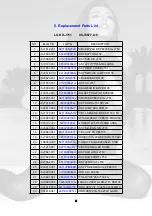
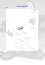
Page 14: ...14 7 Packaging Description 1 JT51 ...

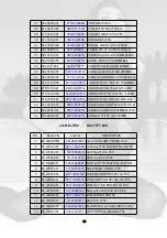
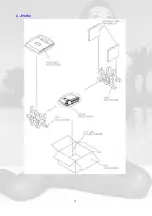
Page 15: ...15 2 JT50 52 ...

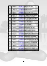
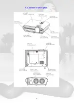
Page 16: ...16 8 Appearance Description ...

Page 17: ...DMD Bias Voltage Alignment Equipment None Procedure Watch DMD Bias Voltage Bin Label Example 8060 7bbc DDDD XXXXXXX M Switch the DIP switch SW2 on Main board according to the red character on the DMD chip 3 00 E 01 D 10 C 11 B ON 0 0 ...

Page 18: ...r decrement the value to let the waveform to be square 9 Do not adjust too much let the signal get ahead if it happens go back to step 7 and do it again 10 Change the input to pure blue and repeat the above procedures again 3 PC Color Alignment Procedure Equipment Pattern generator Procedure 1 Connect power D sub into projector 2 Change pattern generator to pattern 43 5 DISC 3 Light on projector90...

Page 19: ...offset x y Pb offset x y Pb offset x y Pr offset x y Pr offset x y If we line the x and y then the Pb offset is the shift action and the Pr offset is the rotational action 1 Connect power YPbPr Video into projector 2 Change Timing and pattern of pattern generator 3 Timing 480P H 31 54 KHz V 60 08 Hz 4 pattern black 5 Light on projector 6 Set user OSD values to default 7 Enter factory mode 8 Set Fa...

Page 20: ...ocedure 11 Watch DMD chip Label Example 9477000 0234B 12 Switch the DIP switch on DMD board according to the red character on the DMD chip 3 00 B 01 C 10 D 11 E 2 Color Wheel Delay Alignment Equipment Battery Biased Silicon PIN Detector Oscilloscope Probe 0 0 ...

Page 21: ...eform to be square 9 Do not adjust too much let the signal get ahead if it happens go back to step 7 and do it again 10 Change the input to pure blue and repeat the above procedures again 11 Change the input to pure green and repeat the above procedures again 3 Formatter board check procedure Equipment Pattern generator Procedure 1 Connect power D sub into projector 2 Light on projector 3 Testing ...

Page 22: ...step has some pixel lost or can not return it s DMD chip has pixel defect 12 Change to the Slid Line pattern 13 Watch the image if any pixel lost 14 If above step has some pixel lost it s conductive rubber has defect or assembly loosed 5 Optical Engine Assembly Procedure Note Every operator must check the dust chip on every optical component before assembly No Stop Check Action Review Equipment Ch...

Page 23: ... Screw Driver M2 for Clip Light Pipe Chk Concave Mirror Assemble Concave Mirror Instant Glue 460 715 Assemble Assy Fold Mirror Screw Driver M3 Assemble DMD DMD FPC DMD contact Screw Driver M4 for DMD 3 Assy HSG DMD Assemble Club 9 Screw Driver M2 for club 9 Assemble Projection Lens PL contact Screw Driver M3 for PL Assemble HSG DMD Screw Driver for HSG_DMD Assemble HSG CW 4 Assy HSG DMD and HSG CW...

Page 24: ...0 W Pattern Uniformity As per C201 item 1 2 2 Contrast Ratio Checker Board ANSI C R As per C201 item 1 3 R Pattern Chromaticity Coordinate x y As per C201 item 1 5 2 G Pattern Chromaticity Coordinate x y As per C201 item 1 5 3 B Pattern Chromaticity Coordinate x y As per C201 item 1 5 4 Chromaticity Coordinate x y As per C201 item 1 5 1 100 W Pattern Uniformity As per C201 item 1 5 1 3 Color Dark ...

Page 25: ...e video or S Video into projector 2 Change Timing and pattern of pattern generator 3 Timing NTSC H 15 73 KHz V 29 96 Hz 4 Pattern gray 32 or gray16 only for over scan 5 Light on projector 6 Set user OSD values to default 7 Enter factory mode 8 Set Factory values to default 9 Adjust the Brightness and Contrast to let the black level to just distinguish and the light output of white level to just ma...

Page 26: ...ter 1 Pb offset Adjustable CM Red CF1 2 128 128 Pr offset Adjustable CM Green CF1 2 128 128 CM Blue CF1 2 128 128 Red Gain 128 Green Gain 128 Blue Gain 128 White Peak 2 Gamma Table Linear Procedure I Offset adjustment 1 Black coordinate spec Osram lamp Oshio lamp X0 0 281 0 01 0 313 0 01 Y0 0 311 0 01 0 329 0 01 2 The variance of color coordinate via Pb offset and Pr offset X y Pb offset x y Pb of...

Page 27: ...ustment flow chart Example If use the Osram lamp then the x0 0 281 y 0 311 The dash line of x0 and y0 is the target The solid line of x and y is the measured value Case x1 x0 y1 y0 x0 281 y0 311 x 301 y 321 dec Pb x0 281 y0 311 x 291 y 311 dx 01 1 2dx 0 005 dec Pb x0 281 y0 311 x 286 y 306 inc Pr x 281 y 311 x0 281 y0 311 x 291 y 331 dec Pb x0 281 y0 311 x 281 y 321 dy 01 1 2dy 0 005 dec Pb x0 281...

Page 28: ... 271 y 331 dec Pr x0 281 y0 311 x 281 y 321 dy 01 1 2dy 0 005 dec Pb x0 281 y0 311 x 276 y 316 dec Pr x 281 y 311 x0 281 y0 311 x 261 y 321 dec Pr x0 281 y0 311 x 271 y 311 dx 01 1 2dx 0 005 inc Pb x0 281 y0 311 x 276 y 316 dec Pr x 281 y 311 II Gray Level 1 Change Timing and pattern of pattern generator Timing 480P H 31 54 KHz V 60 08 Hz Pattern gray 32 or gray16 only for over scan 2 Adjust the B...

Page 29: ...F1 2 128 128 Green Gain Adjustabl CM Green CF1 2 128 128 Blue Gain Adjustabl CM Blue CF1 2 128 128 Color Temp 0 1 2 White Peak 10 Gamma Table Linear Procedure I Gray Level 1 Connect power D sub or BNC into projector 2 Change Timing and pattern of pattern generator Timing 800x600 60Hz H 37 879Khz V 60 317Hz Pattern gray 32 3 Light on projector 4 Adjust user OSD values to default 5 Enter factory mod...

Page 30: ...Unless other specified all alignments should meet the following conditions 1 All power on and power off condition should be last for more than 5 minute i e no power on is permitted if UUT Unit under test had not been power off and last for more than 5 minute since last power on 2 Brightness and contrast should be measured only 5 minute or more after lamp is on 3 UUT should be placed at a distance ...

Page 31: ...Step PT863 Text EM Character EM distinguish Color Noise Acceptable NTSC H 15 73KHz 29 96Hz I Movie Video Essential Gray 0 100 H V Res 1 Line Color Hue Sat need correct Color Noise Acceptable Smear Not acceptable Linearity As optical spec Composite Video PAL H 15 63KHz 25Hz I PT2 Master Pattern Jitter Swing Snack Ring Cross talk Only Color Noise Acceptable Channel Prime Mode Timing Pattern Item Cri...

Page 32: ... Cross talk Not Acceptable Gray 0 100 H V Res 1 Line Color Hue Sat need correct Smear Not acceptable Linearity As optical spec PT2 Master Pattern Jitter Swing Snack Ring Cross talk Not Acceptable PT976 64Gray Color Gray Color Check 64 Step PT863 Text EM Character EM distinguish NTSC H 15 73KHz 29 96Hz I Movie Video Essential Gray 0 100 H V Res 1 Line Color Hue Sat need correct Smear Not acceptable...

Page 33: ...p H 31 54KHz 60 08Hz p Movie Video Essential Gray 0 100 H V Res 2 Line Color Hue Sat need correct Smear Not acceptable Linearity As optical spec 720p H 45 00KHz 60Hz p PT2 Master Pattern Jitter Swing Snack Ring Cross talk Not Acceptable Gray 0 100 H V Res 4 Line Color Hue Sat need correct Smear Not acceptable Linearity As optical spec YPbPr 1080I H 33 75Khz 30Hz I PT2 Master Pattern Jitter Swing S...

Page 34: ...ear ColorTemp 80 Gray Cool 1 0 272 0 283 0 02 Standard 2 0 281 0 311 0 02 PT46 10 Gray Warm 3 0 313 0 329 0 02 1024 768 85Hz 68 677KHz 84 997Hz Picture Phone Lady Picture check Gray 0 100 H V Res 1 Line Color Hue Sat need correct Smear Not acceptable Linearity As optical spec DSB 640 400 70Hz 31 47KHz 70 08Hz PT2 Master Pattern Jitter Swing Snack Ring Cross talk Not Acceptable Gray 0 100 H V Res 1...

Page 35: ...z PT2 Master Pattern Jitter Swing Snack Ring Cross talk Not Acceptable Gray 0 100 H V Res 1 Line Color Hue Sat need correct Smear Not acceptable Linearity As optical spec 800 600 75Hz 46 875KHz 75Hz PT2 Master Pattern Jitter Swing Snack Ring Cross talk Not Acceptable Gray 0 100 H V Res 2 Line Color Hue Sat need correct Smear Not acceptable Linearity As optical spec 800 600 85Hz 53 67KHz 85 06Hz PT...

Page 36: ...00 Aspect Ratio 4 3 User OSD setting PC 30 gray Final Check Step Screen Check Items Acceptance Criteria Equipment ANSI Lumens 450 PC mode 1 Brightness 100 W Pattern Uniformity 70 2 Contrast Ratio Checker Board ANSI C R 130 1 R Pattern Chromaticity Coordinate x y 0 04 G Pattern Chromaticity Coordinate x y 0 04 B Pattern Chromaticity Coordinate x y 0 04 Chromaticity Coordinate x y 0 04 100 W Pattern...

Page 37: ...s Ring CHK Functionality Adjustable 5 CFM Measure Air Flow TBD CFM Jitter Geometry SMPTE133 Pattern Focus Ring Stuck Bit Color Ramp Pattern Flashing Tint 6 PC Phone Lady picture General Picture Quality PC Flicker Static pattern SMPTE133 Pattern Stuck Bit Tint Noise 7 Video RCA S Video Dynamic movie Toy Story Video Essential General Picture Quality DVD Player 8 Audio Input DVD Player 9 OSD Remote A...

Page 38: ...ing the lamp module The lamp module becomes very hot when the projector is in use DO NOT touch any part of the lamp module that is located in the lamp box Oils from your fingers will cause smudges and uneven heating of lamp surfaces resulting in decreased image quality and premature lamp failure If the lamp is ruptured or the lamp module is cracked or damaged be careful of quartz or glass fragment...

Page 39: ... on the lamp module and pull the module out of the lamp box 2 Covers 1 Remove 5 screws of lower case first 2 Remove 1 screw of each side panel 3 Be sure to remove one wire of keypad board then the upper case can be removed ...

Page 40: ...ìð 4 Then you can remove side panel as well 5 Remove 2 jack screws of rear cover be sure to remove 2 wires as well Then you can take out rear cover The rear cover includes rear fan module ...

Page 41: ...4ï 3 Power Module 1 Remove 4 screws and then take out top mylar 2 Remove 6 wires then you can take out fan board 3 Remove one long screw and one short screw then the whole power module can be removed ...

Page 42: ...wer module includes power board and fan board they can t be separated 4 Ballast 1 Remove 4 screws 2 black screws and 2 sliver screws and one wire 2 Then you can take out ballast as below Fan Board Power Board ...

Page 43: ...ìí 5 Main board 1 Remove one black screw of BKT and then take out it 2 Remove 2 black screws and two wires one is for chip board s connector the other is for AC cable s wire ...

Page 44: ...ìì 3 Remove 4 wires from main board then take out main board 4 Remove 4 screws on the main board module then you can take out main board ...

Page 45: ... 1 Remove one black screw and then blower can be removed from projector 2 Remove 2 screws of blower module and then take out blower 7 Optical engine 1 Remove 3 sliver screws and then optical engine can be removed ...

Page 46: ...ìê 2 Remove 4 screws on the heat sink and then can see chip board and DMD chip 3 Remove 4 screws and then lens can be removed Chip board DMD Chip ...

Page 47: ...ìé 8 Color wheel 1 Remove 2 black screws of color wheel holder 2 Remove 5 screws of color wheel module 9 EMI board 1 Remove 2 long screws one black screw and one wire ...

Page 48: ...screen 2 Use the Keystone correction key on the control panel of the projector or the remote control unit 4 Poor color 1 Select the correct video system 2 Adjust brightness contrast or color 5 Blurred image 1 Press Auto on the control panel of the projector or the remote control unit to get better picture quality 2 Adjust the focus 3 Reposition the unit to improve its projection angle 4 Ensure the...

Page 49: ...Clean DMD 3 Change PL 5 Color Check CW 50 point Replace CW if necessary 6 Color Uniformity Change CM 7 Blue Edge 1 Readjust LP Make sure the LP end is touching with DMD_HSG Datum 2 Check LP If LP is crushed replace with new LP 8 Blue Purple Border 1 Re install SL and AL to ensure correct position 2 Check FM installation 9 Focus 1 Change Projection Lens 2 Put shim metal between upper side of DMD an...

Page 50: ... 66 5 chk U15 soldering 6 change U15 1 chk voltage input from F B 2 5V 5V 12V 2 chk oscillator Y2 Y3 output frequency 16 257MHz 10MHz 3 chk MCLK U24 5 130MHz and DCLK U25 5 40MHz 4 chk U17 whether S W inside or bad soldering 5 change U22 bad soldering 6 chk Reset IC U14 7 chk Abnormal signal 8 chk Resetz RN25 5 Poweron RN25 6 DVS RN18 3 DEN RN18 1 DHS RN18 2 DCLK RN18 4 1 chk output from U15 RN6 R...

Page 51: ...chk bead L710 L714 L44 1 chk clock frequency unit MHz a Y901 30 b Y5 20 C UY1 100 C Motor Controller 8 33 2 chk ACTDATA POWERON RESETZ CLKIN HSYNC VSYNC SYNCVALIDfromFront End 3 chk CW spinning frequency 120Hz if wrong chk MTRDATA MTRCLK MTRSELZ 1 LAMPENSignal to Ballast 2 3 5s after LAMPLIT DMDBecome Activeand Display anImage 1 Output fromDAD1000 VBIAS 22 25V VRST 26V VCC2 7 5V 2 chk control sign...

Page 52: ... time nopulse voltage Yes Yes No No No Rear Front IR function FAN BD Fancontrol 1 chk the voltageof QF1 5 6 7 8 2 chk the fanvoltageU502 2 15 U503 8 3 check Y501 32 768kHz No5V 1 CheckQ701 thermal Breaker LEDdark 1 chk LEDvoltagefromJ1 2 chk the mountingdirectionof LEDs No work 1 chk buttons contact toPCB ...

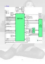
Page 53: ...ëí 5 PFC BOARD 6 DC DC BOARD ...

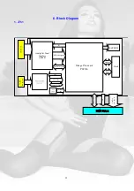
Page 54: ...ëì JT50 52 1 Final Assembly Trouble Shooting Guide ...

Page 55: ...ëë ...

Page 56: ...ëê 2 Engine Assembly Trouble Shooting Guide ...

Page 57: ... u tp u t to P W 1 6 4 B Y e s a C h e c k th e m o u s e o f P C is s till w o rk in g n o rm a lly b C h e c k th e m o u s e d riv e r o f P C is P S 2 c o m p a tib le m o u s e c R e p la c e IR B u ffe r a R e p la c e S P E 2 3 2 E b P W 1 6 4 B a V P X 3 2 2 6 b a d s o ld ie rin g b P W 1 6 4 B b a d s o ld ie rin g c M a in S y s te m b a d c o n n e c tio n a C h e c k th e v o lta g e ...

Page 58: ...ëè 4 Power Supply Trouble Shooting Guide PFC BOARD DX850 DC DC BOARD ...

Page 59: ...5ç 5 DMD Block Trouble Shooting Guide ...

Page 60: ...êð ...

Page 61: ...ctory menu 1 Hold press UP button until the Lamp hours info OSD display on button right of screen Fig 1 Fig 1 Lamp Hours Info 2 Press keypad Menu and Source key simultaneously again then enter Factory menu 2 Factory layer 1 DMD layer Fig 3 Fig 3 DMD layer ...

Page 62: ...rs set this selection to On and system will going to burn in immediately You can see color change red green blue black white on screen in turn System will auto turn off after burn in hour count down to 0 and burn in complete You can also cancel burn in sequence by set this selection to off 2 ADC layer Fig 4 only available when input source is analog RGB Fig 4 ADC layer 1 ADC Brightness ADC brightn...

Page 63: ...bPr Never Change these setting Note these values Before Upgrade Software PbPr G Offset combine with user osd brightness in YPbPr PbPr G Gain combine with user osd contrast in YPbPr PbPr R Offset offset of color red PbPr G Offset offset of color green PbPr R Gain saturation R PbPr B Gain saturation B ...

Page 64: ...while color temp is 11500 11500 B gain of color blue while color temp is 11500 3 3 PC 9300 and Video 9300 9300K submenu Never Change these setting PC 9300 R gain of color red while PC color temp is 9300 PC 9300 G gain of color green while PC color temp is 9300 PC9300 B gain of color blue while PC color temp is 9300 Video 9300 R gain of color red while Video color temp is 9300 Video 9300 G gain of ...

Page 65: ...splay full color green Curtain Blue unit display full color blue 5 Lamp layer Fig 6 Fig 6 Lamp layer Interpolation De interlace Mode Filter system auto select Filter Lamp Hour value to tell you lamp usage hours Usage Hour value to tell you unit usage hours Fac Lamp Hours Record all of the amp usage hours Data Reset Reset all data to default include factory assign value Never try to reset all data ...

Page 66: ...ode is using now Pc PbPr Mode index of input timing RS232 Enable Disable RS232 control 7 FAN Layer T1 DMD DMD sensor temperature T2 Lamp Lamp sensor temperature T3 Blwr Blower sensor temperature F1 Lamp Lamp fan speed in RPM F2 Blst Blaster fan speed in RPM F3 Blwr Blower fan speed in RPM Manual Fan Speed Change fan speed by manual SOG Threshold Change SOG threshold level of AD More Options Change...

Page 67: ...or control testing JT50 52 Activating factory menu I Press and hold keypad Up key for 5 seconds to enter Lamp Life Info state II Press keypad Menu and Source key simultaneously to activate Factory Menu Factory menu details I DMD menu ...

Page 68: ... to the system You can see color changes red green blue black white on screen running in turn System will follow a on off cycle for 2 hours with 5 minute on and 15 minute off After the on off cycle the system will stay on for the rest of the burn in time set in Burn In Hour The system will automatically switch off at the end of the burn in hour expires II ADC menu only available when input source ...

Page 69: ...ideo 9300K color settings for YCbCr S Video Comp Video 6500K color temperature 11500K color settings for 11500K color temperature Mode info detailed for debug only IV Test pattern menu Test Pattern1 2 system generated patterns for engineering test Spoke light displays full white Curtain Red displays full color red Curtain Green displays full color green Curtain Blue displays full color blue ...

Page 70: ... hours Data Reset resets all data to default factory assigned values VI Misc menu Gamma sets Pixelworks gamma index Logo Default Blue Black are the same as in user menu AlwaysBlue AlwaysBlack will remove the logo menu item from user s Setup submenu and set the logo as blue black Interpolation De interlace mode Scaling scaling mode Gray value adjust here to check DMD fail pixel Blue value adjust he...

Page 71: ... speed tachometer values for lamp sensor T1 Blower temperature and fan speed tachometer values for blower sensor Manual Fan Speed Off for normal operation On for thermal engineering FanCal is for blower fan engineering calibration SOG Threshold for debugging only Never change this value More Options for debugging only ...

Page 72: ...T51 Step 1 Setup Flashupgrader in computer Step 2 a Connect download cable with computer and projector b Connect power cord with projector and check power switch is OFF Step 3 Execute Flashupgrader exe Step 4 Setting COM Port Baud Rate ...

Page 73: ...tep 5 a Turn on the power switch of the projector then the Program will target the Flash b HEX File Format choose Intel Extended c File Name choose d Operation choose Program Step 6 Start download firmware ...

Page 74: ...éì Step 7 Download finished Step 8 Turn off the power switch ...

Page 75: ...projector to the COM port on the PC with JT50 JT52 download cable 5 Run FlashUpgrader exe and follow the next step to open the file pwSDK inf You can browse to locate it Select the correct COM port and use 115200 as the BAUD rate 6 When the page with Download progress for the file Flasher HEX shows up turn on the power switch 7 Now the progress bar in the FlashUpgrader should be running 8 Download...

Page 76: ...0 00 00 Force YPbPr BE EF 02 06 00 B3 C7 CA 00 00 00 00 00 RS232 Power ON BE EF 02 06 00 3E C4 D7 00 00 00 00 00 RS232 Power OFF BE EF 02 06 00 C1 C4 D8 00 00 00 00 00 Blank BE EF 02 06 00 1A CC B3 00 00 00 00 00 Operation Packet Type command PC Picture Controls Command Packet Header 7 bytes Packet Payload 25 bytes Brightness BE EF 03 19 00 44 A0 03 C7 02 CC CC 00 00 00 00 CC 16 Brightness BE EF 0...

Page 77: ...Misc Controls Command Packet Header 7 bytes Packet Payload 25 bytes Color Temp 50 0 BE EF 03 19 00 69 49 01 ED 02 CC CC 00 00 00 00 CE FF FF FF CC CC CC CC CC CC CC CC CC CC CC CC 0 10 BE EF 03 19 00 1C 89 01 ED 02 CC CC 00 00 00 00 00 00 00 00 CC CC CC CC CC CC CC CC CC CC CC CC 50 20 BE EF 03 19 00 69 1C 01 ED 02 CC CC 00 00 00 00 32 00 00 00 CC CC CC CC CC CC CC CC CC CC CC CC PIP Controls PIP ...

Page 78: ...DA 02 CC CC 01 00 00 00 03 00 00 00 CC CC CC CC CC CC CC CC CC CC CC CC Video BE EF 03 19 00 DA 74 01 DA 02 CC CC 01 00 00 00 04 00 00 00 CC CC CC CC CC CC CC CC CC CC CC CC PIP Brightness 50 48 BE EF 03 19 00 FE 0B 01 35 02 CC CC 01 00 00 00 CE FF FF FF CC CC CC CC CC CC CC CC CC CC CC CC 0 126 BE EF 03 19 00 8B CB 01 35 02 CC CC 01 00 00 00 00 00 00 00 CC CC CC CC CC CC CC CC CC CC CC CC 50 204 ...

Page 79: ...14 5 4C 3 0 0 0 0 Down 845 JT50 51 BE EF 3 19 0 2 49 5 4D 3 0 0 0 0 Left 846 JT50 51 BE EF 3 19 0 FD AD 5 4E 3 0 0 0 0 Right 847 JT50 51 BE EF 3 19 0 68 F0 5 4F 3 0 0 0 0 Blank 848 JT50 51 BE EF 3 19 0 3D 4C 5 50 3 0 0 0 0 Auto 849 JT50 51 BE EF 3 19 0 A8 11 5 51 3 0 0 0 0 Return 850 JT50 51 BE EF 3 19 0 57 F5 5 52 3 0 0 0 0 Freeze 851 JT50 51 BE EF 3 19 0 C2 A8 5 53 3 0 0 0 0 Power 852 JT50 51 BE...

Page 80: ... 03 19 00 97 14 05 4C 03 00 22 Down BE EF 03 19 00 02 49 05 4D 03 00 22 Left BE EF 03 19 00 FD AD 05 4E 03 00 22 Right BE EF 03 19 00 68 F0 05 4F 03 00 22 Blank BE EF 03 19 00 3D 4C 05 50 03 00 22 Auto BE EF 03 19 00 A8 11 05 51 03 00 22 Return BE EF 03 19 00 57 F5 05 52 03 00 22 Freeze BE EF 03 19 00 C2 A8 05 53 03 00 22 Power BE EF 03 19 00 E8 3E 05 54 03 00 22 Source BE EF 03 19 00 7D 63 05 55 ...

Page 81: ......

Page 82: ...s Optical Points OP OP11 OP OP2 OP OP4 H1 HOLE V8 2 3 4 5 6 7 8 9 H4 HOLE V8 2 3 4 5 6 7 8 9 POWER 01_POWER GND FAN1_E FAN2_B V12 VDD_F SDA SCL OP OP13 OP OP6 OP OP3 OP OP7 FAN 02_FAN GND SDA SCL V12 FAN1_E FAN2_B VDD_F OP OP12 OP OP9 OP OP10 H2 HOLE V8 2 3 4 5 6 7 8 9 OP OP5 H3 HOLE V8 2 3 4 5 6 7 8 9 OP OP1 OP OP8 OP OP14 ...

Page 83: ...V J7302 20L2021005 1 2 3 4 5 CC602 100U 450V C7303 470U 25V C7301 470U 25V CS704 2200P J TP2 CF2 22U 16V L1 500 OHM D6303 US1J 1 2 CA1 0 01U M TP4 C7305 220U 25V J7301 20D0038108 1 1 2 2 3 3 4 4 5 5 6 6 7 7 8 8 R7307 470 CC601 0 47U K C7309 1000P M D7303 SS24 RS702 47 CA2 0 01U M R404 100 D6301 US1M 1 2 PC123FY1 U6302 TP5 TR602 NTC 5 OHM 2 1 3 W T6301 600UH 1 2 4 5 8 9 10 RA603 680K RS701 47 R6301...

Page 84: ...VCC 8 SDA 1 SCL 2 O S 3 C518 220P J R510 10K C501 10P J RA502 5 6K R512 2 4K R501 2M J502 20L2021010 1 2 3 4 5 6 7 8 9 10 Q501 SI4431DY T1 4 R509 2 2K R514 10K C504 0 1U M RB501 2 2K RA503 4 7K Q505 2N3904 1 U501 CD4049UBCM VDD 1 AR 2 A 3 BR 4 B 5 CR 6 C 7 VSS 8 NC 16 FR 15 F 14 NC 13 ER 12 E 11 DR 10 D 9 Q506 2SB772S 3 J501 20L2021004 1 2 3 4 U503 G760A OUT 1 F G 2 ON OFF 3 GND 4 VCC 8 SDA 7 SCLK...

Page 85: ...RST 15 0 P3P3V VCC2 DMDSER DCLK_L LOADB_LZ SACCLK SACBUS SCTRL_L DD 63 0 SACCLK SACBUS SCTRL_L TRC_L LOADB_LZ DCLK_L MBRST 15 0 DMDSER GND VCC2 P3P3V DMD_CHIP DMD_CHIP GND DD 63 0 MBRST 15 0 P3P3V VCC2 DMDSER DCLK_L LOADB_LZ SACCLK SACBUS SCTRL_L TRC_L ...

Page 86: ...TP31 TP65 TP57 TP132 TP28 TP130 J2 20L1065080 2 4 6 8 10 12 14 16 18 20 22 24 26 28 30 32 34 36 38 40 42 44 46 48 50 52 54 56 58 60 62 64 66 68 70 72 74 76 78 80 1 3 5 7 9 11 13 15 17 19 21 23 25 27 29 31 33 35 37 39 41 43 45 47 49 51 53 55 57 59 61 63 65 67 69 71 73 75 77 79 TP111 TP49 TP87 TP63 TP139 TP136 TP115 TP46 TP17 TP128 TP73 TP106 TP47 TP48 TP27 TP36 TP64 TP114 TP58 TP25 R2 1K TP68 TP79 ...

Page 87: ...E29 C3 0 1U M 16V OP OP8 H6 HOLE V8 2 3 4 5 6 7 8 9 C5 0 1U M 16V OP OP11 U1A DMD 0 7XGA DDR MBRST_0 Y10 MBRST_1 AB10 MBRST_2 AA11 MBRST_3 AC11 MBRST_4 AA13 MBRST_5 AC13 MBRST_6 Y14 MBRST_7 AB14 MBRST_8 AB16 MBRST_9 Y16 MBRST_10 AC17 MBRST_11 AA17 MBRST_12 AC19 MBRST_13 AA19 MBRST_14 AB20 MBRST_15 Y20 DCLK C15 LOADB B16 SAC_CLK AC25 SAC_BUS AA25 SCTRL N03 TRC L01 PRG_FUS_EN AC23 BI_MODE Y08 BI_TOF...

Page 88: ... VDD_D SDA SDA0 FAN_P ECO MODE ECO MODE V12_D V DD V DD DRE 7 0 DGE 7 0 DBE 7 0 SCL0 RESETZ POWERON DEN DHS DVS DCLK LAMPLITZ V12_D 2V5_D VDD_D 3 3V_D SDA0 GND LAMPEN ECO MODE VDD PAGE_5 004_DISPLAY 3 3V_D SDA0 SCL0 SDA SCL GND PAGE_4 003_POWER LAMP DETECT GND RESETZ SDA SCL LAMPLITZ LAMPEN VDD_D V12_D 2V5_D 3 3V_D 3 3V VDD ECO MODE FAN_P PAGE_2 001_MAIN 3 3V VDD POWERON RESETZ DRE 7 0 DGE 7 0 DBE...

Page 89: ...nd Ballast for lamp stasus Regect RC1 and RC2 before connect DX660 main board with INTERFACE board PAGE_10 015_PW166 VCLK VFIELD VVS VHS VPEN VY 7 0 GGE 7 0 GRE 7 0 GVS GBLKSPL GHS GFBK GCLK GBE 7 0 GCOAST TDO TXD ROMWEn TCK RXD MCKEXT ROMOEn IRRCVR TMS A 19 1 DCKEXT RESET D 0 15 SDA DVS DHS DRE 7 0 DCLK DGE 7 0 DBE 7 0 A0 BHENn DEN VUV 7 0 POWERON RESETZ DRO 7 0 DGO 7 0 DBO 7 0 SCL VPPEN AUDIO_MU...

Page 90: ...DMD_MOTOR V12_D CKMTR1 EXT ARSTZ MTRSELZ MTRCLK MTRDATA VDD_D CWTACH GND PAGE_15 023_DMD_OSC FAN MOSC GND VDD_D CWINDEX 3 3V_D COSC PAGR_21 029_DMD_CHIP DD 0 63 MBRST 0 15 BINSEL0 BINSEL1 DMDSER LOADB LZ DCLK L VCC2 SACCLK SACBUS SCTRL L TRC L 3 3V_D VDD GND PAGE_14 022_DMD_MEMORY RQ 0 7 DQB 0 8 DQA 0 8 FLASH BUSYZ PUM ARSTZ LAMPLITZ RESETZ POWERON FSD16 DEN DCLK DHS DVS PCLKM SCLKN REFCLK SCK SIO...

Page 91: ...amp on H Lamp off OPEN OPEN L ECO MODE H Normal C9 0 1U 25V Z J704 20D0049108 1 2 3 4 5 6 7 8 R12 2K Q6 MMBT2222A 1 3 2 TP243 R783 10K J702 20D0038108 1 1 2 2 3 3 4 4 5 5 6 6 7 7 8 8 G1 G1 G2 G2 TP241 RC3 10K R711 270 TP250 C828 10U M 20V 1 2 TP247 UL1 74AHC1G08 1 2 3 4 5 RC4 10K C8 0 1U 25V Z L712 80 OHM CP8 0 1U R7 1M Q706 2N3904 1 3 2 R11 100 TP242 TP244 C823 0 1U K C826 0 1U K C7 22U 25V 1 2 C...

Page 92: ...A SCL SCL0 GND SW1 is the switch to choice DDP1000 I2C would be connected with Pixelwork I2C or not J2 is the connector to DDP1000 I2C download by DDP1000 composer OPEN OPEN J2 20L2021003 1 2 3 R19 4 7K TP14 R18 4 7K R16 0 SW1 2240138001 1 1 2 2 3 3 4 4 5 5 6 6 TP15 R21 0 TP16 ...

Page 93: ... DG8 1N4148 1 2 R911 0 TP22 C722 220P J DG13 TZMC5V1 1 2 TP20 U711B 74LVC125A 5 6 4 14 7 DN706 BAV99 1 3 2 RG22 0 RG8 4 7K DG3 BAV99 1 3 2 CG701 0 1U TP29 TP229 TP284 RG4 75 C723 220P J DG703 BAV99 1 3 2 TP23 R796 2K R803 0 R722 3 3K CG3 150P J J821 2210021551 C 4 2 G2 G2 1 Y 3 G1 G1 G3 G3 TP24 J820 2210278001 2 1 G1 G2 CG2 470P K RG6 75 TP17 RG3 75 RG23 0 RG21 0 TP280 R797 1K DG10 TZMC5V1 1 2 RG1...

Page 94: ... AI3D F1 AGNDA L2 AI41 B1 AI42 D2 AI43 D1 AI44 E1 AI4D D3 EXMCLR P3 AOUT M1 VSSA0 M2 VSSA1 J4 VSSA2 H3 VSSA3 E4 VSSA4 C1 VDDA0 M3 VDDA1 K4 VDDA2 H4 VDDA3 F4 VDDA4 D4 VDDA1A L1 VDDA2A J1 VDDA3A G2 VDDA4A E2 VSSD2 D7 VSSD4 D10 VSSD6 F11 VSSD8 J11 VSSD10 L5 VSSD12 L9 VDDD2 C8 VDDD4 C10 VDDD6 F12 VDDD8 J12 VDDD10 M5 VDDD12 M9 VSSD1 D5 VSSD3 D9 VSSD5 D11 VSSD7 G11 VSSD9 L4 VSSD11 L8 VSSD13 L11 VDDD1 C5...

Page 95: ... 15P K C63 0 1U R877 22 RD1 1 5K CA79 0 1U CB81 0 1U C80 0 047U K C883 1 8P J C903 15P K C573 39N K CB84 0 1U RN10 47 1 2 3 4 8 7 6 5 C51 0 1U C65 0 1U R47 47 R812 22 CN6 33P 8 1 7 2 6 3 5 4 CN5 33P 8 1 7 2 6 3 5 4 R792 330 C81 0 1U C54 0 1U C55 0 1U RN8 47 1 2 3 4 8 7 6 5 C53 0 1U RN6 47 1 2 3 4 8 7 6 5 C68 0 1U C56 0 1U C52 0 1U C79 0 047U K UB16 LD1117 3 3V GND 1 VOUT 2 VIN 3 VO 4 C574 3900P K ...

Page 96: ...5 A15 1 A14 2 A13 3 A12 4 A11 5 A10 6 A9 7 A8 8 A17 17 A7 18 A6 19 A5 20 A4 21 A3 22 A2 23 A1 24 A0 25 A16 48 CE 26 OE 28 WE 11 RP 12 WP 14 BYTE 47 A18 16 R90 3 3K SW3 6240019001 1 2 4 3 RB1 10K RA30 3 3K CA30 220P R98 3 3K RB2 47 UI5 74V1G14S 2 4 5 3 1 C330 220P K UI3 74AHC1G32 A 1 B 2 GND 3 VCC 5 Y 4 JP1 20L2055050 1 1 2 2 3 3 4 4 5 5 6 6 7 7 8 8 9 9 10 10 11 11 12 12 13 13 14 14 15 15 16 16 17 ...

Page 97: ...Y5 D9 VY6 C9 VY7 A8 VUV0 B9 VUV1 A9 VUV2 B10 VUV3 A10 VUV4 D11 VUV5 A11 VUV6 C12 VUV7 B13 VCLK D12 VPEN C13 VVS A14 VFIELD A15 VHS B14 C119 0 1U C110 0 1U C113 0 1U R602 2K C111 0 1U RN18 47 1 2 3 4 8 7 6 5 RD5 0 C99 0 1U C117 0 1U R102 2K Misc U22D PW166 10TK A0 P1 A1 P2 A2 N3 A3 N4 A4 R1 A5 R2 A6 T1 A7 T2 A8 R3 A9 U1 A10 U2 A11 R4 A12 T3 A13 V1 A14 W1 A15 V2 A16 T4 A17 U3 A18 Y1 A19 W2 D0 F4 D1 ...

Page 98: ... RK2 RK3 RK4 0ohm ADI RK1 RK2 RK3 RK4 R92 OPEN OPEN OPEN 68 00129 0D1 68 00129 0D1 RK8 0 R115 820K R114 820K U19 XFILT 7 YFILT 6 ST 1 T2 2 VDD 8 COM 3 XOUT 5 YOUT 4 C123 10P D C121 0 1U RK5 O PEN CP6 0 1U 25V Z RK9 4 7K RK3 O PEN C89 0 1U RK2 O PEN U18 G751 2 A2 5 A1 6 A0 7 VCC 8 SDA 1 SCL 2 O S 3 GND 4 L29 Z10 C124 10P D U20 74AHC1G08 1 2 3 4 5 C125 10P D Y3 16 257MHZ R92 O PEN C92 470N M R113 22...

Page 99: ... VCC 20 GND 10 C127 0 1U R813 0 TP232 R744 0 R957 0 TP34 CN701470P 8 1 7 2 6 3 5 4 C812 0 1U TP948 C801 470P K R22 10K C811 0 1U U7 74AHC1G08 1 2 3 4 5 CN703 470P 8 1 7 2 6 3 5 4 L802 240 OHM L801 240 OHM J4 20L2021020 1 2 3 4 5 6 7 8 9 10 11 12 13 14 15 16 17 18 19 20 TP44 TP949 TP233 TP41 R23 510 R958 0 TP35 U28 74LVC273 CLR 1 GND 10 CLK 11 VCC 20 Q1 2 Q2 5 Q3 6 Q4 9 Q5 12 Q6 15 Q7 16 Q8 19 D1 3...

Page 100: ...P5V T22 P2P5V T5 P2P5V R22 P2P5V R5 P2P5V R1 P2P5V M22 P2P5V M5 P2P5V L22 P2P5V L5 P2P5V K22 P2P5V K5 P2P5V E21 P2P5V E20 P2P5V E19 P2P5V E17 P2P5V E16 P2P5V E15 P2P5V E12 P2P5V E11 P2P5V E10 P2P5V E8 P2P5V E7 P2P5V E6 P2P5V B15 GND AF26 GND AF25 GND AF21 GND AF16 GND AF15 GND AF11 GND AF6 GND AF1 GND AE25 GND AE2 GND AE1 GND AD24 GND AD3 GND AC23 GND AC4 GND P5 GND N22 GND N5 GND L26 GND L1 GND J...

Page 101: ...A11 D5 A12 B6 A13 A6 A14 C6 A15 D6 A16 E6 A17 B2 A18 C3 A19 D4 RESET B4 BYTE F6 OE G1 WE A4 CE F1 GND H6 GND H1 VDD G4 NC C4 NC D3 NC B3 TP11 1 C161 0 1U R126 47 TP12 1 R131 39 2F C159 0 1U K R130 10K TP13 1 R125 110F C162 0 1U R127 47 TP9 1 R129 10K R133 39 2F C163 68P J R128 10K RAMBUS JTAG CUSTOMER INPUT U29B DDP1000 C VSYNCZ R26 HSYNCZ N25 WCLK N23 IVALID M23 OLACT M24 SYNCVALID2 DI2 E23 CTRL ...

Page 102: ...0 6 S1 4 OE 7 VDD 2 GND 3 US2 74AHC1G32 A 1 B 2 GND 3 VCC 5 Y 4 C167 10P J Y5 20MHZ C921 0 1U C930 27P J RS1 10K TP54 R918 0 R920 0 RS2 6 8K C170 0 1U R518 0 C926 10P J RS7 2K C909 4 7u RS5 180 C910 27P J Y901 30MHZ 1 3 2 4 C493 22P J RS4 10K RS3 330K U902 CY25812SCT XIN CLKIN 1 VSS 2 S1 3 S0 4 XOUT 8 VDD 7 FRSEL 6 SSCLK 5 R913 39 2F C168 0 1U R927 0 RY1 820K JS1 20L2021003 1 2 3 C169 10P J L16 12...

Page 103: ...7 120 OHM RN32 39 1 2 3 4 8 7 6 5 U31 CDCR83 REFCLK 2 SYNCLKN 7 PCLKM 6 MULT0 15 MULT1 14 S0 24 S1 23 S2 13 PWRDNB 12 STOPB 11 VDDIR 1 VDDIPD 10 CLK 20 CLKB 18 GND 4 GND 5 GND 8 GND 17 GND 21 VDD 3 VDD 9 VDD 16 VDD 22 NC 19 R140 10K C172 0 1U C193 0 1U C181 10U M 6 3V 1 2 C195 0 1U C197 0 1U C175 0 1U R149 39 2F R147 10K R142 56 2F K4R271669D TCS8 RQ0 G1 RQ1 F2 RQ2 F6 RQ3 F7 RQ4 F1 RQ5 E7 RQ6 E6 R...

Page 104: ...38 DD9 DCLK L ADCLK L DMDSER DGE 7 0 DRE 7 0 DBE 7 0 TRC L SCTRL L LOADB LZ SACCLK SACBUS DD 0 63 GND DCLK L ATRC L ADCLK L ALOADB LZ ASCTRL L ATRC L ASACBUS ASACCLK ASACCLK ASACBUS ASCTRL L ALOADB LZ ADCLK L RN40 22 3 4 5 6 14 13 12 11 2 1 7 8 9 10 15 16 RN43 22 3 4 5 6 14 13 12 11 2 1 7 8 9 10 15 16 RN39 22 3 4 5 6 14 13 12 11 2 1 7 8 9 10 15 16 R807 22 C806 10P J RN41 22 3 4 5 6 14 13 12 11 2 1...

Page 105: ... SCPDO 42 SCPENZ 58 STORBE 15 MODE1 2 MODE0 3 SEL1 4 SEL0 5 A3 16 A2 17 A1 18 A0 19 DEV_ID1 45 DEV_ID0 44 RESETZ 59 OEZ 6 VCC 54 V12_SWL1 52 V12_SWL0 51 V12_3 50 V12_2 48 V12_1 11 VBIAS_RAIL7 80 VBIAS_RAIL6 71 VBIAS_RAIL5 70 VBIAS_RAIL4 61 VBIAS_RAIL3 40 VBIAS_RAIL2 31 VBIAS_RAIL1 30 VBIAS_RAIL0 21 VBIAS 9 VBIAS_SWL 8 VBIAS_LHI 10 OUT15 79 OUT14 77 OUT13 74 OUT12 72 OUT11 69 OUT10 67 OUT09 64 OUT0...

Page 106: ...TAIN 23 CD2 2 CWD 3 CD1 24 CRES 12 CST 4 SECDAT 14 FILTER 13 OUTA 5 OUTB 8 OUTC 9 CNTRTAP 10 DATAOUT 17 GNDA 6 GNDB 7 GNDC 18 GNDD 19 R203 1 5 C242 3300P K R194 150 RX4 OPEN R196 150 R201 1K C243 5600P K C233 0 1U M C231 22U 25V 1 2 TP60 C239 1000P K L19 80 OHM RX3 OPEN DN12 BAT54SW 2 1 3 R198 1K C244 3300P K R197 39 2F C237 0 1U K TP58 C245 0 22U K C234 0 1U M DN14 BAT54SW 2 1 3 L20 80 OHM JC1 20...

Page 107: ...Z DCLK L VCC2 SACCLK SACBUS SCTRL L TRC L 3 3V_D VCC2 VDD Optical Points JP2 20L1066080 2 4 6 8 10 12 14 16 18 20 22 24 26 28 30 32 34 36 38 40 42 44 46 48 50 52 54 56 58 60 62 64 66 68 70 72 74 76 78 80 1 3 5 7 9 11 13 15 17 19 21 23 25 27 29 31 33 35 37 39 41 43 45 47 49 51 53 55 57 59 61 63 65 67 69 71 73 75 77 79 OP MARK6 OP MARK3 OP MARK1 OP MARK10 OP MARK9 OP MARK20 OP MARK5 OP MARK15 H3 HOL...

Page 108: ...DRE 7 0 DRE 7 0 SCL0 3 3V_D RESETZ SCL 3 3V_D VDD_D SDA SDA0 FAN_P DRE 7 0 DGE 7 0 DBE 7 0 SCL0 RESETZ POWERON DEN DHS DVS DCLK LAMPLITZ V12_D 2V5_D VDD_D 3 3V_D SDA0 GND LAMPEN DISPLAY 004_DISPLAY 3 3V_D SDA0 SCL0 SDA SCL GND POWER LAMP 003_POWER LAMP DETECT GND RESETZ SDA SCL LAMPLITZ LAMPEN VDD_D V12_D 2V5_D 3 3V_D 3 3V VDD LAMP_P FAN_P MAIN 001_MAIN 3 3V VDD POWERON RESETZ DRE 7 0 DGE 7 0 DBE ...

Page 109: ... RC1 and RC2 the front end I2C bus would be separated with DDP1000 Economy mode switch PW166 015_PW166 VCLK VFIELD VVS VHS VPEN VY 7 0 GGE 7 0 GRE 7 0 GVS GBLKSPL GHS GFBK GCLK GBE 7 0 GCOAST TDO TXD ROMWEn TCK RXD MCKEXT ROMOEn IRRCVR TMS A 19 1 DCKEXT RESET D 0 15 SDA DVS DHS DRE 7 0 DCLK DGE 7 0 DBE 7 0 A0 BHENn DEN VUV 7 0 POWERON RESETZ DRO 7 0 DGO 7 0 DBO 7 0 SCL VPPEN AUDIO_MUT 3 3V CS0n LA...

Page 110: ... VDD_D 2V5_D 3 3V_D VDD_D 2V5_D 3 3V_D VDD_D 3 3V_D V12_D 3 3V_D 3 3V_D 2V5_D From Pixelworks output DMD_MOTOR 027_DMD_MOTOR V12_D CKMTR1 EXT ARSTZ MTRSELZ MTRCLK MTRDATA VDD_D CWTACH GND DMD_OSC FAN 023_DMD_OSC FAN MOSC GND VDD_D CWINDEX 3 3V_D COSC DMD_CHIP 028_DMD_CHIP DD 0 63 MBRST 0 15 BINSEL0 BINSEL1 DMDSER LOADB LZ DCLK L VCC2 SACCLK SACBUS SCTRL L TRC L 3 3V_D VDD_D GND DMD_MEMORY 022_DMD_...

Page 111: ...ff 3 3V for main board 3 3V for DDP1000 LAMPLITZ connected to NPN collection pin and R6 change to 0 ohm Note Generate 10mA and 0 mA current to ballast C9 0 1U 25V Z R12 2K Q6 MMBT2222A 1 3 2 C2 4 7U 35V 1 2 TP8 C5 1U K TP26 RC3 10K C303 0 1U 25V Z UL1 74AHC1G08 1 2 3 4 5 C302 0 1U 25V Z RC4 10K C3 22U 6 3V 1 2 C8 0 1U 25V Z L2 80 OHM CP8 0 1U L8 80 OHM R11 100 TP24 TP14 C1 0 1U 25V Z L5 80 OHM U1 ...

Page 112: ... 3V_D SDA0 SDA SCL SCL0 GND SW1 is the switch to choice DDP1000 I2C would be connected with Pixelwork I2C or not J2 is the connector to DDP1000 I2C download by DDP1000 composer J2 20L2021003 1 2 3 R19 4 7K R18 4 7K R16 0 SW1 2240138001 1 1 2 2 3 3 4 4 5 5 6 6 R21 0 ...

Page 113: ... 2022009024 1 1 2 2 3 3 4 4 5 5 6 6 7 7 8 8 9 9 10 10 11 11 12 12 13 13 14 14 15 15 16 16 17 17 18 18 19 19 20 20 21 21 22 22 23 23 24 24 G1 G1 G2 G2 DN9 TZMC5V1 1 2 UV1 74AHCT1G14 2 4 5 3 1 DG8 TZMC5V1 1 2 RG6 4 7K D3 1N4148 1 2 DN21 1N4148 1 2 DN6 BAV99 1 3 2 R22 10K CG1 0 1U M U11 AT24C02A A0 1 A1 2 A2 3 VSS 4 VCC 8 WP 7 SCL 6 SDA 5 RG5 4 7K DN25 1N4148 1 2 DG9 TZMC5V1 1 2 DN7 BAV99 1 3 2 R23 5...

Page 114: ... L5 VSSD12 L9 VDDD2 C8 VDDD4 C10 VDDD6 F12 VDDD8 J12 VDDD10 M5 VDDD12 M9 VSSD1 D5 VSSD3 D9 VSSD5 D11 VSSD7 G11 VSSD9 L4 VSSD11 L8 VSSD13 L11 VDDD1 C5 VDDD3 C9 VDDD5 D12 VDDD7 H12 VDDD9 M4 VDDD11 M8 VDDD13 M11 VSS xtal A4 VDD xtal B3 XTOUT A2 XTALO A3 XTALI B4 ADP8 P6 ADP7 M6 ADP6 L6 ADP5 N7 ADP4 P7 ADP3 L7 ADP2 M7 ADP1 P8 ADP0 N8 CLKEXT N6 IPD7 K11 IPD6 J13 IPD5 J14 IPD4 H13 IPD3 H14 IPD2 H11 IPD1...

Page 115: ...U K CB82 0 1U C81 0 1U CD1 100P J R77 68 C82 10P J RN8 47 1 2 3 4 8 7 6 5 C78 0 047U K C53 0 1U CA79 0 1U CN6 33P 8 1 7 2 6 3 5 4 U15 AD9882 Rin 70 Gin 65 Bin 59 SOGIN 64 FILT 48 MIDBYPASS 74 REFBYPASS 73 HSYNC 79 VSYNC 80 RX1 36 RX1 35 RX0 33 RX0 32 RXC 41 RXC 42 RX2 39 RX2 38 R_Term 28 CTL0 22 CTL1 23 CTL2 24 CTL3 25 SDA 78 SCL 77 A0 76 GND 1 GND 11 GND 21 GND 26 GND 31 GND 34 GND 37 GND 40 GND ...

Page 116: ...5 1 A14 2 A13 3 A12 4 A11 5 A10 6 A9 7 A8 8 A17 17 A7 18 A6 19 A5 20 A4 21 A3 22 A2 23 A1 24 A0 25 A16 48 CE 26 OE 28 WE 11 RP 12 WP 14 BYTE 47 A18 16 R90 3 3K SW3 6240019001 1 2 4 3 RA30 3 3K RB1 10K CA30 220P R98 3 3K U21 AT24C16N 10SI 1 8 A0 1 A1 2 A2 3 GND 4 VCC 8 WP 7 SCL 6 SDA 5 RB2 47 UI5 74AHC1G14S 2 4 5 3 1 C330 220P K UI3 74AHC1G32 A 1 B 2 GND 3 VCC 5 Y 4 JP1 20L2055050 1 1 2 2 3 3 4 4 5...

Page 117: ...Port U22B PW166 10TK VY0 D8 VY1 C8 VY2 B7 VY3 A7 VY4 B8 VY5 D9 VY6 C9 VY7 A8 VUV0 B9 VUV1 A9 VUV2 B10 VUV3 A10 VUV4 D11 VUV5 A11 VUV6 C12 VUV7 B13 VCLK D12 VPEN C13 VVS A14 VFIELD A15 VHS B14 C105 0 1U C119 0 1U C110 0 1U C113 0 1U TP38 1 RW2 2K R602 2K RN18 47 1 2 3 4 8 7 6 5 C111 0 1U C99 0 1U RD5 0 RX5 1M F R102 2K C117 0 1U RX2 1M F Misc U22D PW166 10TK A0 P1 A1 P2 A2 N3 A3 N4 A4 R1 A5 R2 A6 T...

Page 118: ...4 0ohm ADI RK1 RK2 RK3 RK4 R92 OPEN RK8 0 R115 820K R114 820K U24 ICS511M X1 1 X2 8 CLK 5 S0 6 S1 4 OE 7 VDD 2 GND 3 U19 XFILT 7 YFILT 6 ST 1 T2 2 VDD 8 COM 3 XOUT 5 YOUT 4 C123 10P D C121 0 1U RK5 O PEN CP6 0 1U 25V Z RK9 4 7K RK3 O PEN L28 Z220 C89 0 1U RK2 O PEN U18 G751 2 A2 5 A1 6 A0 7 VCC 8 SDA 1 SCL 2 O S 3 GND 4 C124 10P D L29 Z220 U20 74AHC1G08 1 2 3 4 5 C125 10P D Y3 16 257MHZ R92 O PEN ...

Page 119: ...KEY9 GND VDD 3 3V 3 3V KEY 8 1 KEY 8 1 LED 5 0 LED 5 0 U27 74AHC244 1A1 2 1A2 4 1A3 6 1A4 8 2A1 11 2A2 13 2A3 15 2A4 17 1G 1 2G 19 1Y1 18 1Y2 16 1Y3 14 1Y4 12 2Y1 9 2Y2 7 2Y3 5 2Y4 3 VCC 20 GND 10 C127 0 1U RN81 47 1 2 3 4 8 7 6 5 RN84 47 1 2 3 4 8 7 6 5 J4 20L2021020 1 2 3 4 5 6 7 8 9 10 11 12 13 14 15 16 17 18 19 20 U28 74LVC273 CLR 1 GND 10 CLK 11 VCC 20 Q1 2 Q2 5 Q3 6 Q4 9 Q5 12 Q6 15 Q7 16 Q8...

Page 120: ...10U M 6 3V 1 2 C151 0 1U TP32 1 C139 0 1U C136 10U M 6 3V 1 2 R122 10K C132 0 1U TP31 1 C134 0 1U C143 0 1U R490 47 C152 0 1U TP30 1 L14 120 OHM C147 0 1U C140 0 1U C157 0 1U C149 0 1U R121 10K C130 0 1U C155 0 1U C137 10U M 6 3V 1 2 C135 0 1U C144 0 1U C153 0 1U C128 0 1U U29D DDP1000 C DIO0 R24 DIO1 R23 DIO2 P23 DIO3 R25 DIO4 T24 DIO5 T23 DIO6 U26 DIO7 T25 DIO8 U24 DIO9 V26 DIO10 U23 DIO11 U25 D...

Page 121: ...A11 D5 A12 B6 A13 A6 A14 C6 A15 D6 A16 E6 A17 B2 A18 C3 A19 D4 RESET B4 BYTE F6 OE G1 WE A4 CE F1 GND H6 GND H1 VDD G4 NC C4 NC D3 NC B3 C161 0 1U TP11 1 R126 47 TP12 1 R131 39 2F C159 0 1U K R130 10K TP13 1 R125 110F C162 0 1U R127 47 TP9 1 R129 10K R133 39 2F C163 68P J R128 10K RAMBUS JTAG CUSTOMER INPUT U29B DDP1000 C VSYNCZ R26 HSYNCZ N25 WCLK N23 IVALID M23 OLACT M24 SYNCVALID2 DI2 E23 CTRL ...

Page 122: ... 2 GND 3 US2 74AHC1G32 A 1 B 2 GND 3 VCC 5 Y 4 C410 0 1U RS6 75K Y5 20MHZ C167 10P J TP16 U503 CY25812SCT XIN CLKIN 1 VSS 2 S1 3 S0 4 XOUT 8 VDD 7 FRSEL 6 SSCLK 5 RS1 10K RS2 6 8K C170 0 1U TP18 C411 0 1U C412 12P J RS7 2K Y503 30MHZ 1 3 2 4 RS5 180 TP17 R413 39 2F C493 22P J C413 12P J RS4 10K RS3 330K C168 0 1U RY1 820K L407 120 OHM JS1 20L2021003 1 2 3 C169 10P J R136 39 2F L16 120 OHM L27 Z220...

Page 123: ...NCLKN 7 PCLKM 6 MULT0 15 MULT1 14 S0 24 S1 23 S2 13 PWRDNB 12 STOPB 11 VDDIR 1 VDDIPD 10 CLK 20 CLKB 18 GND 4 GND 5 GND 8 GND 17 GND 21 VDD 3 VDD 9 VDD 16 VDD 22 NC 19 R140 10K C172 0 1U C193 0 1U C181 10U M 6 3V 1 2 C195 0 1U C197 0 1U C175 0 1U RN33 39 F 1 2 3 4 8 7 6 5 R149 39 2F R147 10K K4R271669D TCS8 RQ0 G1 RQ1 F2 RQ2 F6 RQ3 F7 RQ4 F1 RQ5 E7 RQ6 E6 RQ7 E2 SIO1 J3 SIO0 J5 CTM E1 CTMN D1 CFM ...

Page 124: ...1 Y2 DD42 Y3 DD43 W4 DD44 W2 DD45 Y1 DD46 W3 DD47 V4 DD48 V2 DD49 W1 DD50 V3 DD51 U2 DD52 U4 DD53 V1 DD54 U3 DD55 U1 DD56 T4 DD57 T3 DD58 R2 DD59 P4 DD60 R3 DD61 R4 DD62 P2 DD63 P1 A0 C25 A1 D24 A2 E24 A3 C26 A4 D25 A5 E25 A6 F23 A7 D26 A8 F25 A9 F24 B0 G23 B1 E26 B2 G25 B3 G24 B4 H23 B5 H25 B6 G26 B7 H24 B8 J23 B9 J25 C0 H26 C1 J24 C2 K23 C3 J26 C4 K24 C5 L25 C6 K26 C7 L23 C8 L24 C9 M25 DCLK_L AE...

Page 125: ...EL1 4 SEL0 5 A3 16 A2 17 A1 18 A0 19 DEV_ID1 45 DEV_ID0 44 RESETZ 59 OEZ 6 VCC 54 V12_SWL1 52 V12_SWL0 51 V12_3 50 V12_2 48 V12_1 11 VBIAS_RAIL7 80 VBIAS_RAIL6 71 VBIAS_RAIL5 70 VBIAS_RAIL4 61 VBIAS_RAIL3 40 VBIAS_RAIL2 31 VBIAS_RAIL1 30 VBIAS_RAIL0 21 VBIAS 9 VBIAS_SWL 8 VBIAS_LHI 10 OUT15 79 OUT14 77 OUT13 74 OUT12 72 OUT11 69 OUT10 67 OUT09 64 OUT08 62 OUT7 39 OUT6 37 OUT5 34 OUT4 32 OUT3 29 OU...

Page 126: ...P K C233 0 1U M C231 22U 25V 1 2 C239 1000P K U42 A8904SLB VBB 1 VDD 15 BRAKEZ 11 OSC 16 RESETZ 20 CSZ 21 CLOCK 22 DATAIN 23 CD2 2 CWD 3 CD1 24 CRES 12 CST 4 SECDAT 14 FILTER 13 OUTA 5 OUTB 8 OUTC 9 CNTRTAP 10 DATAOUT 17 GNDA 6 GNDB 7 GNDC 18 GNDD 19 L19 80 OHM RX3 OPEN DN12 BAT54SW 2 1 3 R198 1K C244 3300P K R197 39 2F C237 0 1U K C245 0 22U K C234 0 1U M DN14 BAT54SW 2 1 3 L20 80 OHM JC1 20K2002...

Page 127: ...Z DCLK L VCC2 SACCLK SACBUS SCTRL L TRC L 3 3V_D VCC2 VDD_D Optical Points H4 HOLE V8 1 2 3 4 5 6 7 8 9 OP MARK11 OP MARK13 JP3 20L1066080 2 4 6 8 10 12 14 16 18 20 22 24 26 28 30 32 34 36 38 40 42 44 46 48 50 52 54 56 58 60 62 64 66 68 70 72 74 76 78 80 1 3 5 7 9 11 13 15 17 19 21 23 25 27 29 31 33 35 37 39 41 43 45 47 49 51 53 55 57 59 61 63 65 67 69 71 73 75 77 79 OP MARK14 OP MARK6 OP MARK10 O...

Page 128: ... 2K TP7 TP15 J1 20L2021020 1 2 3 4 5 6 7 8 9 10 11 12 13 14 15 16 17 18 19 20 LED8 BLUE A K TP4 SW4 6940046001 1 3 2 4 SW6 6940046001 1 3 2 4 R48 2K R2 2K Q1 2N3904 1 3 2 LED7 BLUE A K R23 150 R15 2K R45 22 R11 130 C5 680P 50V J TP14 R43 22 TP10 R9 130 D9 RED GRN 3 4 2 1 SW9 6940046001 1 3 2 4 TP6 C8 680P 50V J R20 10K TP8 C3 680P 50V J TP2 LED1 BLUE A K Q7 2N3904 1 3 2 SW2 6940046001 1 3 2 4 R8 1...

Page 129: ...crew Holes OP OP3 H4 HOLE V8 1 2 3 4 5 6 7 8 9 OP OP4 OP OP7 OP OP8 OP OP13 OP OP12 OP OP10 H2 HOLE V8 1 2 3 4 5 6 7 8 9 H3 HOLE V8 1 2 3 4 5 6 7 8 9 OP OP9 H5 HOLE V8 1 2 3 4 5 6 7 8 9 OP OP6 OP OP5 OP OP14 OP OP1 OP OP11 H1 HOLE V8 1 2 3 4 5 6 7 8 9 OP OP2 ...

Page 130: ...ical Points OP OP11 OP OP2 OP OP4 H1 HOLE V8 1 2 3 4 5 6 7 8 9 H4 HOLE V8 1 2 3 4 5 6 7 8 9 POWER 01_POWER GND FAN1_E FAN2_B V12 VDD_F SDA SCL OP OP13 OP OP6 OP OP3 OP OP7 FAN 02_FAN GND SDA SCL V12 FAN1_E FAN2_B VDD_F OP OP12 OP OP9 OP OP10 H2 HOLE V8 1 2 3 4 5 6 7 8 9 OP OP5 H3 HOLE V8 1 2 3 4 5 6 7 8 9 OP OP1 OP OP8 OP OP14 ...

Page 131: ...2 4 7 3 1 6 5 8 TP1 1 QF1 SI4431DY T1 2 4 7 3 1 6 5 8 U6305 PQ1CY1032Z GND 3 VOUT 2 VIN 1 ON 5 FB 4 G 6 CS702 1000P K RF5 1K C6301 0 01U M CA1 0 01U M D6303 US1J 1 2 J6301 2062010103 1 2 3 R7304 5 1K TP2 1 3 W T6301 600UH 1 2 4 5 8 9 10 R6307 47 C7309 1000P M CC601 0 47U K U6301 TOP247Y C 1 F 5 X 3 S 4 D 7 L 2 W2 IN 1 CS703 2200P J R701 47K R7309 2 32KF C6303 47U 50V 1 2 R6304 30K CA2 0 01U M D630...

Page 132: ...R510 10K R7 10K C501 10P J R512 2 4K J502 20L2021010 1 2 3 4 5 6 7 8 9 10 R501 2M C6 1U 50V Z R514 10K R509 2 2K RA503 4 7K RB501 2 2K Q505 2N3904 1 3 2 Q506 2SB772S 3 1 2 U501 CD4049UBCM VDD 1 AR 2 A 3 BR 4 B 5 CR 6 C 7 VSS 8 NC 16 FR 15 F 14 NC 13 ER 12 E 11 DR 10 D 9 J501 20L2021004 1 2 3 4 R511 2 4K Y501 25 6KHZ RA501 4 7K C507 2200P K R11 5 1K MAX6660AEEE U3 VFAN 1 VCC 2 STBY 15 SMBCLK 14 SMD...

Reviews: