LG-
K
D3500
LGE
LG Electronics Inc.
14/21
1. RF Transmit/Receive Part
1.1 Overview
The RF transmit/receive part employs the direct conversion architecture (ZIF, Zero Intermediate
Frequency). The transmit/receive frequency is respectively 824.04~848.97MHz and 869.04~893.97
MHz. The block diagram is shown in [Figure 3-1].
RF signals received through the antenna are fed QSC6010 through the duplexer. And then, they pass
the low noise amplifier (LNA), combined with the signals of local oscillator (VCO) at the frequency
mixer in order to create baseband signal directly.
Baseband signals created are changed into digital signals by the analog / digital converter (ADC, A/D
Converter) and then, auto gain controlled and, are demodulated by the modulator / demodulator.
In the case of transmission, QSC6010 modulates, interpolates, and converts the digital signal into an
analog baseband before upconverts the Tx analog baseband into RF.
The baseband quadrature signals are upconverted to the Cellular Tx frequency bands and amplified to
provide signal drive capability to the power amp.
After that, the RF signal is amplified by the Power Amp in order to have enough power for radiation.
Finally, the RF signal is sent out to the cell site via the antenna after going through the duplexer
CHAPTER 3. Circuit Description
Summary of Contents for RD3500
Page 2: ...CDMA MOBILE SUBSCRIBER UNIT LG KD3500 SINGLE BAND CDMA MOBILE PHONE SERVICE MANUAL ...
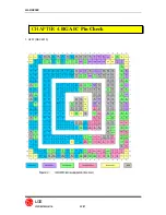
Page 24: ...LG KD3500 LGE LG Electronics Inc 22 21 1 U201 QSC6010 CHAPTER 4 BGA IC Pin Check ...
Page 25: ...LG KD3500 LGE LG Electronics Inc 23 21 2 U310 Memory ...
Page 28: ...Circuit Diagram DP101 DP101 ...
Page 36: ...4 3 2 Charging Trouble Test Points Circuit Diagram CON409 CON409 pin1 ...
Page 47: ...4 3 10 LCD Trouble Test Points Circuit Diagram C O N 3 0 4 CON304 pin3 ...
Page 50: ...CON302 Test Points Circuit Diagram 4 3 11 UIM Trouble R375 R378 R361 R376 ...
Page 54: ......
Page 55: ......
Page 56: ......
Page 57: ......
Page 60: ......
Page 73: ......

