LG-
K
D3500
LGE
LG Electronics Inc.
15/21
[Figure 3-1] Block Diagram Of RD3500
1.2 Description of Receive Part Circuit
1.2.1 Duplexer (DP101)
The duplexer consists of the receive part bandpass filter (BPF) and the transmit part bandpass filter
(BPF) which have the function of separating transmit/receive signals in the full duplex system using
the transmit/receive common antenna. The transmit part BPF is used to suppress noises and spurious
waves entering the receive band among transmit signals in order to prevent the drop in receive
sensitivity characteristics. The receive part BPF blocks the signals sent out from entering the receive
end in order to improve sensitivity characteristics.
Insertion loss (IL) in the transmit band is 2.8dB (Max), whereas IL in the receive band is 3.5dB (Max).
The receive band attenuation amount of transmit filter is 45dB (Min) and the transmit band attenuation
amount of receive filter is 57dB or more (Min).
TX
RX
DUP
ANT
BPF
DC 5V
Battery
19.2M OSC
Keypad
Backlight
MCP
32Mb X 16Mb
LCD
Backlight
Viblator
SPK/Earpiec
MIC
Keypad
User
Memory
Codec
SPK AMP
RF
Interface
Input
General
BB & PM
I/F
Output
Connectivity
UIM
USB
Quadrature
Quadrature
LN
RF Block
BPF
RD3500 Block Diagram
QSC6010
Summary of Contents for RD3500
Page 2: ...CDMA MOBILE SUBSCRIBER UNIT LG KD3500 SINGLE BAND CDMA MOBILE PHONE SERVICE MANUAL ...
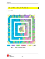
Page 24: ...LG KD3500 LGE LG Electronics Inc 22 21 1 U201 QSC6010 CHAPTER 4 BGA IC Pin Check ...
Page 25: ...LG KD3500 LGE LG Electronics Inc 23 21 2 U310 Memory ...
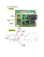
Page 28: ...Circuit Diagram DP101 DP101 ...
Page 36: ...4 3 2 Charging Trouble Test Points Circuit Diagram CON409 CON409 pin1 ...
Page 47: ...4 3 10 LCD Trouble Test Points Circuit Diagram C O N 3 0 4 CON304 pin3 ...
Page 50: ...CON302 Test Points Circuit Diagram 4 3 11 UIM Trouble R375 R378 R361 R376 ...
Page 54: ......
Page 55: ......
Page 56: ......
Page 57: ......
Page 60: ......
Page 73: ......

