background image

SERVICE MANUAL

SERVICE MANUAL

CAUTION

BEFORE SERVICING THE UNIT, READ THE “SAFETY PRECAUTIONS”
IN THIS MANUAL.

CONFIDENTIAL

MODEL: SL8YG (SL8YG, SPL8-W)

P/NO : AFN78474486

FEBRUARY, 201

9

MODEL:  SL8YG

(SL8YG, SPL8-W)

Copyright © 2019 LG Electronics Inc. All rights reserved. 
Only for training and service purposes. 

Wi-Fi Sound Bar

Summary of Contents for SL8YG

Page 1: ... THE UNIT READ THE SAFETY PRECAUTIONS IN THIS MANUAL CONFIDENTIAL MODEL SL8YG SL8YG SPL8 W P NO AFN78474486 FEBRUARY 2019 MODEL SL8YG SL8YG SPL8 W Copyright 2019 LG Electronics Inc All rights reserved Only for training and service purposes Wi Fi Sound Bar ...

Page 2: ...ectronics Inc All rights reserved Only for training and service purposes CONTENTS SECTION 1 GENERAL SECTION 2 CABINET MAIN CHASSIS SECTION 3 ELECTRICAL SECTION 4 WIRELESS SUBWOOFER PART SECTION 5 WIRELESS RECEIVER PART OPTION ...

Page 3: ...INES FOR AUDIO PRODUCTS 1 3 SERVICING PRECAUTIONS 1 4 GENERAL SERVICING PRECAUTIONS INSULATION CHECKING PRODEDURE ELECTROSTATICALLY SENSITIVE ES DEVICES NAME OF EACH COMPONENT 1 5 WIRELESS SUBWOOFER CONNECTION 1 7 REAR SPEAKERS CONNECTION SOLD SEPARATELY 1 8 WOOFER REAR PAIRING METHOD 1 9 HIDDEN KEY MODE 1 10 SOFTWARE UPDATE GUIDE 1 11 SPECIFICATIONS 1 14 ...

Page 4: ...ign Be sure that the safety purpose of the polarized line plug has not been defeated 3 Soldering must be inspected to discover possible cold solder joints solder splashes or sharp solder points Be certain to remove all loose foreign particles 4 Check for physical evidence of damage or deterioration to parts and components for frayed leads or damaged insulation including the AC cord and replace if ...

Page 5: ... more than 1Mohm Note 1 Accessible Conductive Parts include Metal panels Input terminals Earphone jacks etc Electrostatically Sensitive ES Devices Some semiconductor solid state devices can be damaged easily by static electricity Such components commonly are called Electrostatically Sensitive ES Devices Examples of typical ES devices are integrated circuits and some field effect transistors and se...

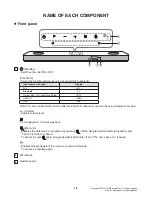
Page 6: ... Wired LG TV HDMI IN HDMI USB USB Note You can use Bluetooth function after making Wi Fi network connection by using Google Home app Volume Adjusts volume level Starts playback Pauses playback Mic mute Disables the detect voice recognition by pressing All the Google Assistant LED turns amber and The mic is muted is heard To cancel it press again Google Assistant LED turns off and The mic is back o...

Page 7: ...ect the OPTICAL IN jack on the back of the unit to OPTICAL OUT jack on the TV USB Port Connect USB memory device to the USB port on the back of the unit 1 3 2 4 5 Google Assistant LED Changes LED status according to Google Assistant performance LED Status Description All four LEDs are on Ready to listen to your voice command All four LEDs blink Responds to your voice command Microphone is off and ...

Page 8: ...ubwoofer does not make sound To solve the problem follow the steps below 1 Press Pairing on the rear of the wireless subwoofer The green LED on the rear of the wireless subwoofer blinks quickly If the green LED does not blink press and hold the Pairing 2 Turn on the sound bar 3 Pairing is completed Pairing is completed The green LED on the rear of the wireless subwoofer turns on Note It takes a fe...

Page 9: ... Color Status Yellow green Blink The connection is trying Yellow green The connection is completed Red The wireless receiver is in standby mode or the connection is failed Off No display The power cord of wireless receiver is disconnected Setting up the wireless receiver for the first time 1 Connect the power cord to the wireless receiver to the outlet 2 Turn on the main unit The sound bar and wir...

Page 10: ...out 2 3 seconds on Remocon and then will display WL RESET on LCD 3 Press paring key on the Subwoofer and Rear kit 4 When woofer and rear kit attempt to connect wireless the Green color LED blink faster than standby status 5 When woofer and rear kit connect wireless completely the LED will maintain Green color WOOFER REAR PAIRING METHOD Remocon Rear kit front Mute Key Paring Key Standby LED Subwoof...

Page 11: ...TX Woofer TX RX Woofer RX D DSP H HDMI RR Rear RX RT Rear TX T Touch L Sub MICOM MICOM DSP PEQ 3 Option Change Soundbar Volume key and Remocon for 3 seconds B skip and F Skip can change Option Number Play Pause key can change Option Value Remocon Info key can save a modified Option and Reboot 4 Woofer Rear Speaker Reset Soundbar Volume key and Remocon MUTE for 3sec Volume must be Min 0 before inpu...

Page 12: ...x_xxxxxxx BIN WOOFER RX WOOFERRX_SLx_xxxxxxx BIN REAR TX REARTX_SLx_xxxxxxx BIN REAR RX REARRX_SLx_xxxxxxx BIN DSP DSP_SLx_xxxxxxx wav HDMI HDMI_SLx_xxxxxxx bin 1 2 Update Steps 1 Create UPDATE Folder in USB root Folder 2 Copy all update files to UPDATE folder 3 After Soundbar Booting finish insert USB 4 Check REMOVE USB on VFD 5 Detach USB VFD display WIFI for a second and system will reboot auto...

Page 13: ...onics Inc All rights reserved Only for training and service purposes 2 Using APP Before Network update soundbar has to be connected with LG Wifi Soundbar Application Step 1 Select setting gui Step 2 Select software version display ...

Page 14: ... training and service purposes Using APP Step 3 System compare current version with the latest version at server Step 4 If there is new version on server press Update Step 6 Updating Step 7 After update finish application show the result Step 5 Update file downloading ...

Page 15: ...ut Total 440 W RMS Front 50 W RMS x 2 4 Ω at 1 kHz THD 10 Center 40 W RMS 4 Ω at 1 kHz THD 10 Top 40 W RMS x 2 4 Ω at 1 kHz THD 10 Subwoofer 220 W RMS 3 Ω at 80 Hz THD 10 WIRELESS SUBWOOFER Power requirements Refer to the main label on the subwoofer Power consumption Refer to the main label on the subwoofer Type 1 Way 1 Speaker Impedance 3 Ω Rated Input Power 220 W RMS Max Input Power 440 W RMS Di...

Page 16: ...and service purposes SECTION 2 CABINET MAIN CHASSIS CONTENTS DISASSEMBLY INSTRUCTIONS 2 2 1 HOW TO DISASSEMBLE THE MAIN UNIT 2 2 2 HOW TO DISASSEMBLE THE SUBWOOFER 2 6 EXPLODED VIEWS 2 9 1 MAIN UNIT SECTION 2 9 2 WIRELESS SUBWOOFER SECTION 2 11 3 PACKING ACCESSORY SECTION 2 13 ...

Page 17: ...EMBLE THE MAIN UNIT Figure 1 1 1 1 Disassemble of Case Bottom Disassemble Red points Screw 1SSZR 0097X 24EA Disassemble Screw 1SSZR 0097X 24 EA Figure 1 2 1 1 2 Disassemble Main PCB and Frame 1 Disassemble Case 4 Point Figure 1 2 2 2 Disassemble Screw 2 Point Disassemble Red points Screw 1SSZR 0098H 2EA Disassemble Screw 1SSZR 0098H 2EA ...

Page 18: ...hts reserved Only for training and service purposes HOW TO DISASSEMBLE THE MAIN UNIT Figure 1 3 1 3 Disassemble Chamber Figure 1 4 1 4 Disassemble Main PCB and AMP PCB Disassemble Red points Screw 1SSZR 0098H 3EA Disassemble Screw 1SSZR 0098H 3EA ...

Page 19: ...1 5 1 1 5 Disassemble PCB 1 Disassemble Front PCB Screw Disassemble Red points Screw 1SSZR 0098H 2EA Disassemble Screw 1SSZR 0098H 2EA Figure 1 5 2 2 Disassemble Main PCB and Amp PCB Disassemble Cable 4 Point of red mark Figure 1 6 1 6 Disassemble DSP PCB Disassemble Screw 4 Point of red mark Disassemble Red points Screw 1SSZR 0098H 4EA ...

Page 20: ...LE THE MAIN UNIT Figure 1 7 1 1 7 Disassemble Main PCB Disassemble screw 2 Point of red mark Figure 1 7 2 Disassemble Red points Screw 234 022S 2EA Figure 1 8 1 8 Disassemble of Module Holders Wi Fi BT Holder Wireless Rear Wireless Disassemble screw 3 Point of red mark Disassemble Red points Screw 1SSZR 0098H 3 EA ...

Page 21: ... reserved Only for training and service purposes Rear Panel Assembly SPK cable Figure 2 1 1 Figure 2 1 2 2 HOW TO DISASSEMBLE THE SUBWOOFER 2 1 Rear Panel Assembly 1 Remove the 11 screws 2 Pull out the Rear Panel Assembly and disconnect the SPK cable ...

Page 22: ...dule 1 Disconnect the FFC cable 2 Remove the EVA sheet 0 15T covered the WIRELESS module 3 Remove the WIRELESS module 4 Remove the EVA gasket 1 0T covered the WIRELESS module Caution when assembling the WIRELESS Module 1 Attach the EVA gaskets 1 0T to both sides of the WIRELESS module 2 Assemble the WIRELESS module into the wireless holder 3 Attach the EVA sheet 0 15T to the WIRELESS module 4 Conn...

Page 23: ... rights reserved Only for training and service purposes 1 2 Figure 2 3 1 Figure 2 3 2 HOW TO DISASSEMBLE THE SUBWOOFER 2 3 AMP SMPS PCB Assembly 1 Disconnect the Power inlet socket cable 2 Remove the 5 screws 3 Remove the AMP SMPS PCB Assembly ...

Page 24: ...ing and service purposes 2 10 2 9 A K C D J F H A80L G B A80R A80C A42 I WIRELESS FRONT WIRELESS WI FI CABLE5 MPEG MAIN AMP H G K J I C D E F B A CABLE2 CABLE3 CABLE4 A43 LCD801 A54 A54 263 A47 262 262 A51 266 A46 A48 A41 L E L CABLE1 EXPLODED VIEWS 1 MAIN UNIT SECTION ...

Page 25: ...Copyright 2019 LG Electronics Inc All rights reserved Only for training and service purposes 2 12 2 11 2 WIRELESS SUBWOOFER SECTION B A 954 951 A45W A B A54W 953 961 A900 ...

Page 26: ...ctronics Inc All rights reserved Only for training and service purposes 806 Optical cable 300 Power cord 833 AC adapter 836 Screws 2 835 Wall bracket 900 Remote control 829 Cable tie 3 3 PACKING ACCESSORY SECTION 837 Holder foot ...

Page 27: ...2 14 Copyright 2019 LG Electronics Inc All rights reserved Only for training and service purposes ...

Page 28: ...WHEN YOU TURN THE UNIT ON NO MESSAGE OR HELLO ON FRONT PANEL 3 5 2 NO SOUND 3 9 3 PROTECTION ERROR 3 13 WAVEFORMS OF MAJOR CHECK POINT 3 16 1 CRYSTAL 3 15 2 REMOTE CONTROL 3 19 3 OPTICAL 3 20 CIRCUIT VOLTAGE CHART 3 21 1 ICs 3 21 2 CAPACITORS 3 24 3 CONNECTORS 3 24 PRINTED CIRCUIT BOARD DIAGRAMS 3 25 1 MAIN P C BOARD DIAGRAM 3 25 2 DSP P C BOARD DIAGRAM 3 27 3 AMP P C BOARD DIAGRAM 3 29 4 FRONT LE...

Page 29: ...105 CN601 CN702 CN703 CN704 99999 CNF01 CNF01 12P BtoB 14P FFC CN103 26P BtoB DSP FR4 Epoxy 4layer 1 4T 120x70mm CN606 CN606 30P BtoB CN210 CN607 26P FFC CNM01 MIC TOUCH FR4 Epoxy 2layer 1 6T 135x42mm 26P FFC 12P FFC FRONT FR4 Epoxy 2layer 1 6T 81x33 8mm 26P FFC 12P Harness AMP DC JACK Wi Fi BT Combo Module Wireless Rear Module Wireless Woofer Module CN209 CN208 CN207 JK201 JK200 JK601 WIRING DIAG...

Page 30: ... N DSP_C WF DAT K D D D D D D DSP 19x19mm 0 8p 349 BGA 1 1 1 5 3 3 V DDR3 128 MB S Flash 16 MB Downmix 2ch M M M M M M M C HDMI 1 0 3 3 V S S S S S S Flash 1 MB SPI S Flash 1 MB SPI IR Receiver LCD 5Digit LCD_CLK D0 STB BL_CTL LED Mic Touch Key TOUCH_CTRL Adapter PVDD 25 V LED PCB M M DIR 3 3 V SPI SYS Power PM IC MICOM 3 3VA 100p DDR3 512 MB eMMC 4 GB A A TUNER 3 3 V FM ANT FM OPTION Not included...

Page 31: ...3 Switch 500 mA USB_5 V USB IC315 Switch 50 mA VCC5 V LCD ADC TUNER IC207 Switch 91 mA HDMI_5VA HDMI IC604 DCDC 2 A 240 mA MICOM TOUCH IC607 Switch IC503 DDR3 IC603 DDR3 DSP_3 3 V 100 mA DSP_1 5 V 400 mA IC606 LDO IC317 Switch IC318 Switch WIRELESS Woofer 5G WIRELESS Rear 5G WLS_3V3 65 mA 65 mA RBOX_3V3 HD 3 3 V IC803 Switch IC319 Switch IC611 Switch IC320 LDO NET_3 3V 356 mA 103 mA 42 mA AEC IC U...

Page 32: ...D A 6 0 1 R A 6 0 0 R A 6 0 1 6 0 4 0 R 7 5 3 D S P _ S R _ S L R A 6 1 5 R A 6 1 6 R A 6 1 7 R 7 5 7 R A 6 1 8 R A 6 1 9 C A 6 4 1 A R 6 0 6 A R 6 0 7 A R 6 0 8 F 6 0 1 F 6 0 2 R A 6 2 0 C A 6 5 3 C A 6 5 4 C A 6 5 7 C A 6 5 8 C A 6 5 9 C A 6 6 0 C A 6 6 3 C A 6 6 6 C A 6 6 7 C A 6 6 8 C A 6 7 8 R A 6 5 7 C A 6 8 0 R A 6 5 8 C A 6 8 1 R A 6 5 9 R A 6 6 5 C A 6 9 2 C A 6 9 3 C A 6 9 4 7YG R A 6 7 ...

Page 33: ... 1 F 8 7 R 1 G 6 R 1 G 7 C 4 3 5 C 4 3 7 R 1 H 0 R 1 H 1 R 1 H 2 R 1 H 3 R 1 H 4 R 1 H 5 R 1 H 6 R 1 H 7 R 1 H 8 R 1 H 9 C 4 4 7 C 4 5 3 R 1 J 0 R 1 J 1 R 1 J 2 R 1 J 3 R 1 J 4 R 1 J 7 C 3 F 5 R 1 K 1 R 1 K 2 I C 2 0 4 T P 1 7 5 T P 1 7 6 L 3 1 0 I C 4 0 2 I C 4 0 3 C 3 H 5 C 3 H 6 C 3 H 7 C 3 H 8 C 3 H 9 R 1 N 1 R 1 N 2 R 1 N 3 F B 1 0 2 F B 1 0 3 N 9 R 1 0 0 R 1 0 1 R 1 0 2 R 1 0 3 R 1 0 4 R 1 0...

Page 34: ...rd 1 3 3 Service hint Any picture Remark MAIN board top view F B 4 1 4 R 2 1 0 R 2 1 1 R 2 1 2 R 2 1 3 R 2 1 4 R 2 1 5 R 2 1 6 C N 2 0 3 R 3 A 4 R 3 A 5 R 3 A 8 R 1 B 7 R 1 B 8 R 1 C 7 R 1 D 0 R 2 5 4 R 2 5 7 R 2 5 8 R 3 E 7 C 5 A 1 C L 5 0 1 C 5 A 8 B 6 C 3 B 7 R 4 6 R 4 6 7 R 4 6 8 R 4 6 9 R 4 7 7 R 4 7 8 R 4 7 9 C 5 C 1 C 5 C 3 R 4 8 0 R 4 8 1 R 4 8 2 R 4 8 3 R 4 8 4 R 4 8 5 Q 1 0 2 C 2 6 0 C 2...

Page 35: ...is abnormal replace MAIN board 3 If PMCI_4 1 V is OK replace FRONT board 1 4 3 Service hint Any picture Remark MAIN board top view F B 4 1 4 R 2 1 0 R 2 1 1 R 2 1 2 R 2 1 3 R 2 1 4 R 2 1 5 R 2 1 6 C N 2 0 3 R 3 A 4 R 3 A 5 R 3 A 8 R 1 B 7 R 1 B 8 R 1 C 7 R 1 D 0 R 2 5 4 R 2 5 7 R 2 5 8 R 3 E 7 C 5 A 1 C L 5 0 1 C 5 A 8 B 6 C 3 B 7 R 4 6 R 4 6 7 R 4 6 8 R 4 6 9 R 4 7 7 R 4 7 8 R 4 7 9 C 5 C 1 C 5 C...

Page 36: ... I N T R 2 2 0 R 2 2 1 R 2 2 2 R 2 2 3 C N 2 0 7 R 2 2 4 R 2 2 5 C N 2 0 9 R 2 2 6 R 2 2 7 R 2 2 8 F B 8 1 5 R 2 2 9 R 5 A 9 R 2 3 1 R 2 3 2 R 2 3 3 R 2 3 4 R 2 3 5 R 2 3 6 R 2 3 7 R 2 3 8 C 2 0 2 C 2 0 3 C 2 0 4 C 2 0 5 C 2 0 7 C 2 0 9 R 8 2 7 C 2 1 0 X 2 0 1 R 8 2 9 C 2 1 4 C 2 1 5 C 2 1 6 C 2 1 7 C 2 1 8 C 2 1 9 R 8 3 1 R 8 3 5 R 8 3 6 R 8 3 7 C 2 2 0 C 2 2 2 C 8 0 0 C 8 0 4 R 8 4 2 R 8 4 3 R 8...

Page 37: ...C 8 7 3 C 8 7 7 C 8 8 0 I C 8 0 0 I C 8 0 2 C 8 8 3 C 8 8 8 R 5 M D E M O _ S P D I F C 8 9 1 C 8 9 4 F B 3 1 5 F B 3 1 7 R 2 A 5 R 2 A 6 R 2 C 3 R 3 3 6 C 3 0 3 C 3 0 4 C 3 C 3 P 2 C 2 A 1 C 2 A 2 R 3 6 0 C 3 4 4 R 2 H 1 C 3 4 9 A R 8 1 0 A R 8 1 1 A R 8 1 2 A R 8 1 3 Z D 2 0 1 R R 3 R 3 R 3 R C 3 7 5 C 3 7 6 C 3 7 7 C 3 7 8 F L 2 0 1 F L 2 0 2 F L 2 0 3 F L 2 0 4 F L 2 0 5 C 3 8 6 F L 2 0 6 C 2 ...

Page 38: ... 7 3 C 8 7 7 C 8 8 0 I C 8 0 0 I C 8 0 2 C 8 8 3 C 8 8 8 D E M O _ S P D I F C 8 9 1 C 8 9 4 F B 3 0 4 F B 3 1 5 R 2 A 5 R 3 1 5 R 2 A 6 R 3 1 6 R 3 1 8 R 3 1 9 R 1 3 0 R 2 C 3 R 2 C 8 C 3 P 2 C 3 2 0 C 3 2 1 C 3 2 2 C 3 2 3 C 3 2 4 R C 3 2 6 C 2 C 1 C 2 C 2 C 2 C 3 C 2 C 4 A R 8 0 1 A R 8 0 2 A R 8 0 3 A R 8 0 4 C 3 4 2 C 3 4 3 R 2 H 1 A R 8 1 0 A R 8 1 1 A R 8 1 2 A R 8 1 3 Z D 2 0 1 R 3 9 1 D 3...

Page 39: ... 0 I C 8 0 0 I C 8 0 2 C 8 8 3 C 8 8 8 R 5 M D E M O _ S P D I F C 8 9 1 C 8 9 4 F B 3 1 5 F B 3 1 7 R 2 A 5 R 2 A 6 R 2 C 3 R 3 3 6 C 3 0 3 C 3 0 4 C 3 C 3 P 2 C 2 A 1 C 2 A 2 R 3 6 0 C 3 4 4 R 2 H 1 C 3 4 9 A R 8 1 0 A R 8 1 1 A R 8 1 2 A R 8 1 3 Z D 2 0 1 R R 3 R 3 R 3 R C 3 7 5 C 3 7 6 C 3 7 7 C 3 7 8 F L 2 0 1 F L 2 0 2 F L 2 0 3 F L 2 0 4 F L 2 0 5 C 3 8 6 F L 2 0 6 C 2 H 6 F L 2 0 7 I C 3 0...

Page 40: ... I C 6 1 3 P D A T C A 6 0 0 C A 6 0 2 C A 6 0 3 C A 6 0 4 R 7 3 4 R 7 3 6 C A 6 2 0 R A 6 0 0 R A 6 0 1 R A 6 0 4 R A 6 0 5 R A 6 0 6 R A 6 1 0 D S P _ S R _ S L R A 6 1 5 R A 6 1 6 R A 6 1 7 R A 6 1 8 R A 6 1 9 C A 6 4 1 A R 6 0 6 A R 6 0 7 A R 6 0 8 R A 6 2 0 C A 6 8 0 C A 6 8 1 C A 6 9 2 C A 6 9 3 R7YG R A 6 7 8 R7YY SL8Y SL8YG C 7 A 0 C 7 A 1 C 7 A 2 C 7 A 3 C 7 A 6 C 7 A 7 T L _ N T L _ P T ...

Page 41: ...4 L 7 0 1 L 7 0 2 L 7 0 5 L 7 0 6 L 7 0 8 R 7 0 0 R 7 0 1 R 7 0 2 R 7 0 4 R 7 0 5 R 7 0 6 R 7 0 7 R 7 0 8 R 7 0 9 R 7 1 0 R 7 1 1 R 7 1 2 R 7 1 3 R 7 1 5 R 7 1 9 Q A 6 0 3 R 7 2 0 Q A 6 0 4 R 7 2 1 R 7 2 2 R 7 2 3 R 7 2 4 R 7 2 5 R 7 2 6 R 7 2 7 R 7 3 8 C 7 0 4 R 7 4 0 C 7 0 5 R 7 4 2 C 7 0 6 C 7 0 7 R 7 4 3 C 7 0 8 C 7 1 0 C 7 1 1 C 7 1 2 C 7 1 4 C 7 1 5 R 7 5 1 R 7 5 2 C 7 1 7 R 7 5 4 C 7 1 8 C ...

Page 42: ... 1 5 R 7 1 9 Q A 6 0 3 R 7 2 0 Q A 6 0 4 R 7 2 1 R 7 2 2 R 7 2 3 R 7 2 4 R 7 2 5 R 7 2 6 R 7 2 7 R 7 3 8 C 7 0 4 R 7 4 0 C 7 0 5 R 7 4 2 C 7 0 6 C 7 0 7 R 7 4 3 R 7 4 4 C 7 0 8 C 7 1 0 C 7 1 1 C 7 1 2 C 7 1 4 C 7 1 5 R 7 5 1 R 7 5 2 C 7 1 7 R 7 5 4 C 7 1 8 C 7 1 9 R 7 5 5 R 7 5 6 R 7 5 8 C 7 2 0 C 7 2 1 C 7 2 2 C 7 2 3 C 7 2 5 C 7 2 6 C 7 2 8 C 7 2 9 C 7 3 1 C A 6 5 5 C A 6 5 6 C 7 3 3 C 7 3 9 C 7...

Page 43: ...service purposes 1 26MHz X500 1 X TAL1 2 GND 3 X TAL2 4 GND DGND C558 NC WAVEFORMS OF MAJOR CHECK POINT 1 CRYSTAL Fig 1 2 Crystal X800 27 MHz Fig 1 1 Crystal X500 26 MHz 1 2 2 X800 27MHz 1 INPUT OUTPUT 2 FLOAT 3 INPUT OUTPUT 4 FLOAT R829 1M R831 0 R827 1 8K DGND C804 10pF C800 15pF ...

Page 44: ...z X201 1 X TAL 2 GND 3 X TAL 4 GND R218 NC R224 0 R223 0 DGND DGND C203 27pF C202 27pF CRYSTAL Fig 1 4 Crystal X603 12 288 MHz Fig 1 3 Crystal X201 24 576 MHz 3 4 4 SG 310SCN 12 288MHz X603 1 ST 2 GND 3 OUT 4 VCC DSP_3 3V C616 10nF DGND DGND R672 33 12 288Mhz R670 10K FB601 220 C635 10nF 12 288Mhz Oscillator ...

Page 45: ...602 0 R676 680 C682 8pF C683 8pF DGND BMODE0 BMODE1 BMODE2 DSP_RST 25MHZ X601 1 HOT 2 GND 3 HOT 4 GND X602 24 576MHz 1 INPUT OUTPUT 2 FLOAT 3 INPUT OUTPUT 4 FLOAT R604 10K R619 10K C684 100nF R677 1K R689 0 NC R690 0 NC ZD601 Z02W3 9V 1 2 3 DGND R693 0 Close to IC501 7 CA600 8pF CA620 8pF RA601 1M RA600 2 2K DGND XA601 24 576MHz 1 INPUT OUTPUT 2 FLOAT 3 INPUT OUTPUT 4 FLOAT Fig 1 7 Crystal XA601 2...

Page 46: ... ZDF01 Z02W3 9V 1 2 3 RCF01 AO R123C7G LG T GND VCC VOUT GND CF01 10uF DGND 3 3VA CF02 100nF RMC 2 REMOTE CONTROL Fig 2 2 Remote Control High Timing Fig 2 1 Remote Control Input Voltage 8 Fig 2 3 Remote Control Low Timing 10 9 Item Measured Spec Input Level 3 3 V IR Receiver Spec 2 7 5 5 V Low Timing 4 4 ms 3 6 ms 5 04 ms High Timing 4 48 ms 4 08 ms 5 04 ms ...

Page 47: ...ce purposes 12 11 OPTICAL JACK 192KHz OPT_IN OPT_DET M_OPT_IN 3 3VA R2C4 100 R2C2 560 R2C1 33 R2C3 100 JK201 1 VOUT 2 GND 3 VCC FB215 PZ1608U221 1R4TF DGND DGND C285 10uF C286 100nF C292 100pF C287 15pF MPEG MICOM OPTICAL DIR 3 OPTICAL Fig 3 2 Optical Opt Det Fig 3 1 Optical Opt In 11 12 ...

Page 48: ... IC103 SERIAL FLASH MEMORY VCC 8 Spec VCC 2 7 3 6 V Measured VCC 3 36 V IC203 Vcc 20 Spec Vcc 2 0 5 5 V Measured Vcc 3 36 V IC206 Analog Switch VDD 10 Spec VCC 2 5 3 6 V Measured VCC 3 36 V IC207 Switch IC Vin 5 Vout 1 Spec Vin 2 5 5 5 V Out 0 5 5 V Measured Vin 5 15 V Vout 5 15 V IC302 DC DC Vin 1 SW 2 Spec Vin 4 2 17 V Out 0 8 10 V Measured Vin 12 1 V Out 5 15 V IC309 DC DC Vin 4 SW 3 Spec Vin 2...

Page 49: ...0 PVDD10 CVDD10 Spec AVDD33 3 14 3 46 V IOVCC33 3 14 3 46 V SBVCC5V 4 5 5 5 V R 0 2 PWR5V 4 5 5 5 V XTALVCC33 3 14 3 46 V AVDD10 1 0 1 1 V PVDD10 1 0 1 1 V CVDD10 1 0 1 1 V Measured AVDD33 3 35 V IOVCC33 3 35 V SBVCC5V 5 03 V R 0 2 PWR5V 5 09 V XTALVCC33 3 35 V AVDD10 1 03 V PVDD10 1 03 V CVDD10 1 03 V IC901 Microcontrollers VCC 48 Spec VCC 2 7 5 5 V Measured VCC 3 36 V IC Capacitive Touch Sensor ...

Page 50: ... C 5 0 2 C 5 8 2 I C 5 0 3 C 5 8 3 I C 5 0 4 C 5 8 4 F L 2 1 0 L 8 0 1 I C 3 1 1 C 5 8 6 I C 3 1 2 I C 3 1 4 D S P _ I 2 S _ S R _ S L I C 3 1 5 I C 3 1 6 R 2 M 3 C 3 9 8 S W 2 0 0 I C 3 1 8 R 2 M 4 I C 3 1 9 I C 3 2 0 C 2 J 3 C 2 J 4 C 5 9 8 C 2 J 5 C 5 9 9 C 2 J 6 F B 2 0 3 F B 2 0 4 F B 2 0 6 J K 2 0 0 J K 2 0 1 F B 4 0 1 R 2 0 1 F B 4 0 6 R 2 0 2 R 2 0 3 R 2 0 4 F B 2 1 5 E A X 6 8 8 0 5 6 0 2...

Page 51: ... 8 R 6 J 4 C 6 F 9 R 6 J 5 R 6 J 6 R 6 J 7 R 6 J 8 L 6 0 1 R 6 J 9 L 6 0 2 L 6 0 5 C 6 G 1 C 6 G 2 C 6 G 3 C 6 G 4 C 6 G 5 R 6 K 1 C 6 G 6 R 6 K 2 C 6 G 7 C 6 G 8 R 6 K 5 C 6 G 9 D S P _ I 2 S _ S R _ S L R 6 K 8 R 6 K 9 C 6 H 1 C 6 H 2 C 6 H 3 C 6 H 5 C 6 H 6 C 6 H 7 C 6 H 8 C 6 J 1 C 6 J 2 C 6 J 3 C 6 J 4 C 6 J 5 C 6 J 6 C 6 J 7 C 6 J 8 C 6 J 9 F B 6 0 2 F B 6 0 3 SL8 DSP EAX68322901 Ver1 5 FR4 ...

Page 52: ...K 1 2 D S P _ I 2 S _ F R _ t r 1 1 D S P _ I 2 S _ F L _ t l 1 0 G N D 9 G N D 8 P W R _ C T R L 7 K E Y 6 3 3 V A 5 P W R _ G D 4 G N D 3 G N D 2 1 2 V 1 1 2 V SL8Y SL8YG 1 8 2 3 4 7 6 5 J K 6 0 1 F B 6 2 3 F B 6 2 6 F B 6 2 7 C N 6 0 1 T P 7 0 0 T P 7 0 1 T P 7 0 2 T P 7 0 3 T P 7 0 4 C 7 A 4 C 7 A 5 T P 7 0 5 T P 7 0 6 T P 7 0 7 T P 7 1 0 T P 7 1 1 Z D 7 0 1 Z D 7 0 2 Z D 7 0 4 L 7 0 1 L 7 0 2...

Page 53: ...1 2 R M 1 3 R M 1 4 R M 1 5 R M 1 6 R M 1 7 M _ D A T R M 1 8 R M 1 9 C N M 0 1 R M 2 0 R M 2 1 R M 2 2 R M 2 3 5 V 1 A P W R C M 0 1 C M 0 2 C M 0 3 C M 0 4 C M 0 5 C M 0 6 C M 0 7 C M 0 8 C M 0 9 C M 1 0 C M 1 1 C M 1 2 C M 1 3 C M 1 4 C M 1 5 C M 1 6 C M 1 7 C M 1 8 C M 1 9 C M 2 0 SL8 MIC TOUCH EAX68403402 Ver1 1 FR4 4L 1 4T 2019 01 08 135 X 47 F B F 0 1 F B F 0 2 R F 0 3 R F 0 4 R F 0 5 R F 0...

Page 54: ...NTENTS WIRING DIAGRAM 4 2 BLOCK DIAGRAM 4 3 ONE POINT REPAIR GUIDE 4 4 1 POWER ON ERROR 4 4 2 WIRELESS CONNECTION 4 6 WAVEFORMS OF MAJOR CHECK POINT 4 7 1 CRYSTAL 4 7 2 FLASH MEMORY 4 7 3 VOLTAGE 4 8 4 AMP VOLTAGE 4 9 5 PWM 4 10 6 LED 4 11 CIRCUIT VOLTAGE CHART 4 13 PRINTED CIRCUIT BOARD DIAGRAMS 4 15 1 WOOFER SMPS AMP P C BOARD 4 15 ...

Page 55: ... 2 Copyright 2019 LG Electronics Inc All rights reserved Only for training and service purposes 2P 3 96mm ST Non Lock SMD 26P 0 5mm ST Non Lock SMD Wireless 2P 3 96mm ST Non Lock SMD Power WIRING DIAGRAM ...

Page 56: ...ht 2019 LG Electronics Inc All rights reserved Only for training and service purposes PWM IC Wireless TX Wireless RX FL LPF AMP IC FR LPF AMP_PDN SW SW AMP_SD I2S I2C Reset KEY PAIRING LED RED GREEN BLOCK DIAGRAM ...

Page 57: ...9 W R 9 1 5 W R 9 1 8 W T H 9 0 1 W C 7 0 0 W C 9 0 0 W C 9 0 5 W R 7 5 0 W R 7 5 1 W R 7 5 5 W R 7 5 6 W C 7 4 7 W C 9 4 0 W C 7 7 0 W C 7 7 2 W C 7 7 4 W I C 9 0 5 W Z D 9 0 3 W F L 9 0 1 T P 1 9 T T P 2 T P 3 3 T P W W R 9 W R 9 W R 9 4 3 W R 9 4 4 W C 9 1 3 B B B S P L 5 E A X B L W B R C A U T I O N R I S K O F F I R E R E P L A C E F U S E A S M A R K E D T 5 A H 2 5 0 V W R 7 6 5 W C 7 6 4 ...

Page 58: ... W C 6 1 7 W C 6 2 0 W C 6 2 1 WPW901 W Q 7 0 2 W Q 7 0 3 W Q 7 0 4 W Q 7 0 5 Q 7 0 7 W I C 6 0 1 W R 7 0 0 W R 7 0 1 W R 7 2 2 W R 7 2 4 W R 7 2 6 W R 7 3 3 R 7 3 4 5 W C 7 0 7 W C 7 0 8 W C 7 0 9 W C 7 1 0 W C 7 1 1 G N D B C K A M P _ S D P _ S E N S E W F 9 0 1 Z D 7 0 1 W V 9 0 1 W F L 9 0 2 L R C K P W M _ R S T WIC703 WIC703 ONE POINT REPAIR GUIDE POWER ON ERROR Fundamental power check poin...

Page 59: ... R E R E P L A C E F U S E A S M A R K E D T 5 A H 2 5 0 V W R 7 6 4 W R 7 6 5 W R 7 7 4 W C 7 6 2 W C 7 6 4 W C 7 6 6 W C 7 6 7 W I C 7 0 5 W C 7 9 0 W C 7 9 2 W F B 6 0 1 W F B 6 0 2 W F B 6 0 3 W F B 6 0 4 W R 6 0 3 W R 6 0 4 W C N 6 0 1 W R 6 2 1 W R 6 2 2 W R 6 2 5 W R 6 2 6 W R 6 2 7 W R 6 2 8 W R 6 2 9 W R 6 3 0 W R 6 3 1 W R 6 3 2 W R 6 3 3 W R 6 3 4 W R 6 3 5 W R 6 3 6 W R 6 3 7 W R 6 3 8...

Page 60: ...2019 LG Electronics Inc All rights reserved Only for training and service purposes WAVEFORMS OF MAJOR CHECK POINT 1 CRYSTAL 2 FLASH MEMORY FIG 1 WX601 24 576 MHz FIG 2 VCC CS CLK DO 1 2 4 3 5 VCC CS CLK DO 1 2 4 5 3 ...

Page 61: ...Copyright 2019 LG Electronics Inc All rights reserved Only for training and service purposes 3 VOLTAGE FIG 3 2 Woofer 12 VA FIG 3 1 Woofer PVDD 6 7 FIG 3 3 Woofer 3 3 VA 8 FIG 3 4 Woofer 3 3V_PWM 9 7 6 8 9 ...

Page 62: ...4 9 Copyright 2019 LG Electronics Inc All rights reserved Only for training and service purposes 4 AMP VOLTAGE FIG 4 2 AMP_12V FIG 4 1 AMP PVDD 10 11 11 10 ...

Page 63: ...4 10 Copyright 2019 LG Electronics Inc All rights reserved Only for training and service purposes 5 PWM FIG 5 2 Woofer PWM SW Signal FIG 5 1 Woofer PWM SW Signal 12 13 13 12 ...

Page 64: ...4 11 Copyright 2019 LG Electronics Inc All rights reserved Only for training and service purposes 6 LED FIG 6 2 Pairing On Status Green LED FIG 6 1 Pairing Off Status Red LED 14 15 15 14 ...

Page 65: ...4 12 Copyright 2019 LG Electronics Inc All rights reserved Only for training and service purposes ...

Page 66: ... VDD_PLL 1 08 V 1 32 V 1 28 V 1 28 V WIC701 IC Audio Amplifier PVDD 29 30 31 36 37 38 PVDD 12 V 34 V 20 61 V 20 64 V GVDD 1 22 GVDD 10 8 V 13 2 V 12 41 V 12 42 V VDD 2 VDD 10 8 13 2V 12 47 V 12 47 V WIC703 IC Analog Switch VIN 1 VIN 2 8 V 5 5 V 3 42 V 3 42 V VOUT 6 VOUT 2 8 V 5 5 V 3 41 V 3 41 V WIC704 IC DC DC Converter VIN 7 VIN 4 5 V 45 V 34 61 V 34 64 V SW 1 VOUT 0 8 V 42 V 12 53 V 12 53 V WIC...

Page 67: ...9 4 0 W C 9 4 7 W D 9 0 2 W C 7 7 0 W C 7 7 2 W C 7 7 4 W H S 9 0 1 W H S 9 0 2 W I C 9 0 4 W I C 9 0 5 W T 9 0 1 W D 9 2 6 W D 9 2 7 W C 7 9 4 W F 9 0 1 W Z D 9 0 2 W Z D 9 0 3 W V 9 0 1 W C M 9 0 1 W B C 9 0 4 W Q 9 1 1 W Q 9 1 2 W F L 9 0 1 W F L 9 0 2 T P 1 9 T P 2 1 T P 2 2 T P 3 3 W R 9 0 1 W R 9 0 2 W R 9 0 3 T P 4 2 W R 9 1 1 W R 9 1 2 W R 9 1 3 W R 9 1 4 W R 9 1 6 W R 9 2 1 W R 9 2 7 W R ...

Page 68: ...e purposes SECTION 5 WIRELESS RECEIVER PART OPTION CONTENTS WIRING DIAGRAM 5 2 BLOCK DIAGRAM 5 3 ONE POINT REPAIR GUIDE 5 4 ELECTRICAL TROUBLESHOOTING GUIDE 5 5 WAVEFORMS 5 7 PRINTED CIRCUIT BOARD DIAGRAMS 5 9 1 WIRELESS RECEIVER SMPS P C BOARD 5 9 2 WIRELESS RECEIVER AMP P C BOARD 5 11 ...

Page 69: ...Copyright 2019 LG Electronics Inc All rights reserved Only for training and service purposes Rear AMP SMPS Wireless RCN301 CN901 RJK301 SPK RR RL 26P FFC R C N 3 0 3 10P Harness SPK terminal WIRING DIAGRAM ...

Page 70: ...ght 2019 LG Electronics Inc All rights reserved Only for training and service purposes PWM IC Wireless TX Wireless RX RL LPF AMP RR LPF AMP_PDN RL RR AMP_SD I2S I2C R Reset KEY PAIRING LED RED GREEN BLOCK DIAGRAM ...

Page 71: ...easure 2 How to Duplicate Problem Wireless rear speaker doesn t output a sound 2 1 Solution Replace AMP board No 12 V 2 2 How to troubleshoot Countermeasure 2 3 Service hint Any picture Remark Check LED color of RX BOX Try to remate or reset Color is yellow Replace SMPS board YES NO RIC307 RIC307 RIC308 RIC308 RIC307 RIC308 AMP board top view NO Replace AMP board Check 3 3 V YES Replace SMPS board...

Page 72: ...less rear speaker doesn t output a sound 3 1 Solution Replace AMP board No 3 3 V 3 2 How to troubleshoot Countermeasure 3 3 Service hint Any picture Remark RIC307 RIC307 RIC308 RIC308 RIC307 RIC308 AMP board top view NO Replace AMP board Check Module or connection YES Replace SMPS board 5 VA RIC307 pin2 no input PWM 3 3 V RIC307 pin3 no output YES NO ...

Page 73: ...r Connection Yellow LED blinks irregularly Sound cut off irregularly Red LED is turned on LED is Red Turn off the equipment that gives interference Turn off the equipment that gives interference interference interference Remate Remate Check SMPS board AMP PVDD RCN301 pin9 10 no output Check RIC308 AMP 12 V RIC308 pin4 no output Check RIC307 3 3 V RIC307 pin3 no output YES YES YES YES YES YES YES N...

Page 74: ... 7 Copyright 2019 LG Electronics Inc All rights reserved Only for training and service purposes RCN303 pin1 I2S LRCK RCN303 pin3 I2S BCK 1 2 WAVEFORMS 1 AUDIO PART I2S RCN303 pin20 I2S Audio Data 3 3 1 2 ...

Page 75: ...5 8 Copyright 2019 LG Electronics Inc All rights reserved Only for training and service purposes ...

Page 76: ...l rights reserved Only for training and service purposes PRINTED CIRCUIT BOARD DIAGRAMS 1 WIRELESS RECEIVER SMPS P C BOARD TOP VIEW BOTTOM VIEW 5 9 5 10 NOTE Warning Parts that are critical with respect to risk of fire or electrical shock ...

Page 77: ...Copyright 2019 LG Electronics Inc All rights reserved Only for training and service purposes 5 11 5 12 2 WIRELESS RECEIVER AMP P C BOARD TOP VIEW BOTTOM VIEW ...

Reviews: