- 8/132-
LG Electronics Inc.
3. Structure and Functions of tri-band CDMA Mobile Phone
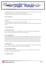
The hardware structure of CDMA mobile phone is made up of radio frequency (RF) part and logic part. The RF part
is composed of Receiver part (Rx), Transmitter part (Tx) and Local part (LO). For the purpose of operating on tri-
band, It is necessary dual Tx path, tri Rx path, dual PLL and switching system for band selection. The mobile phone
antenna is connected with the frequency separator which divide antenna input/output signals between Cellular
frequency band (824~894 MHz) and PCS frequency band (1850~1990MHz). Each separated path is linked with the
Cellular duplexer and PCS duplexer. Duplexer carries out separating Rx band and Tx band. The Rx signals from the
antenna are converted into intermediate frequency(IF) band by the frequency synthesizer and frequency down
converter. And then, pass SAW filter which is a band pass filter for removing out image frequency. The IF output
signals that have been filtered is converted into digital signals via Analog-to-Digital Converter (ADC). In front of the
ADC, switching system is required to choose which band path should be open. The digital signals send to 5
correlators in each CDMA de-modulator. Of these, one is called a searcher whereas the remaining 4 are called data
receivers (fingers). Digitalized IF signals include a great number of call signals that have been sent out by the
adjacent cells. These signals are detected with pseudo-noise sequence (PN Sequence). Signal to interference ratio
(C/I) on signals that match the desired PN sequence are increased through this type of correlation detection process,
but other signals obtain processing gain by not increasing the ratio. The carrier wave of pilot channel from the cell
site most adjacently located is demodulated in order to obtain the sequence of encoded data symbols. During the
operation with one cell site, the searcher searches out multi-paths in accordance with terrain and building reflections.
On three data receivers, the most powerful 3 paths are allocated for the parallel tracing and receiving. Fading
resistance can be improved a great deal by obtaining the diversity combined output for de-modulation. Moreover, the
searcher can be used to determine the most powerful path from the cell sites even during the soft handoff between the
two cell sites. Moreover, 3 data receivers are allocated in order to carry out the de-modulation of these paths. Output
data that has been demodulated changes the data string in the combined data row as in the case of original
signals(deinterleaving), and then, are demodulated by the forward error correction decoder which uses the Viterbi
algorithm.
Mobile station user information send out from the mobile station to the cell site pass through the digital voice
encoder via a mike. Then, they are encoded and forward errors are corrected through the use of convolution encoder.
Then, the order of code rows is changed in accordance with a certain regulation in order to remove any errors in the
interleaver. Symbols made through the above process are spread after being loaded onto PN carrier waves. At this
time, PN sequence is selected by each address designated in each call.
Signals that have been code spread as above are digital modulated (QPSK) and then, power controlled at the
automatic gain control amplifier (AGC Amp). Then, they are converted into RF band by the frequency synthesizer
synchronizing these signals to proper output frequencies.
Transmit signals obtained pass through the duplexer filter and then, are sent out to the cell site via the antenna.
Z3X-BOX.COM
Summary of Contents for VX9700
Page 26: ... 25 132 LG Electronics Inc VX9700 28 Powering Down Restart Z 3 X B O X C O M ...
Page 59: ... 58 132 LG Electronics Inc VX9700 Waveform Waveform F106 pin2 DP2 pin2 Z 3 X B O X C O M ...
Page 154: ...CON104 Z 3 X B O X C O M ...
Page 156: ...Z 3 X B O X C O M ...
Page 159: ...CON809 SW101 SW102 Z 3 X B O X C O M ...
Page 160: ...CON808 Z 3 X B O X C O M ...
Page 162: ...CON809 SW104 Z 3 X B O X C O M ...
Page 163: ...CON808 Z 3 X B O X C O M ...
Page 165: ...SW1 CON2 Z 3 X B O X C O M ...
Page 166: ...CON1 Z 3 X B O X C O M ...
Page 167: ... 15 132 LG Electronics Inc VX9700 Appendix 3 Part List VX9700 Part List Z 3 X B O X C O M ...
Page 168: ... 16 132 LG Electronics Inc VX9700 Appendix 4 Components Layout Z 3 X B O X C O M ...
Page 174: ...Z 3 X B O X C O M ...

