
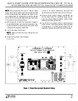

QUICK START GUIDE FOR DEMONSTRATION CIRCUIT 1317A-A
ACTIVE RESET ISOLATED 48V INPUT TO 3.3V @30A DC/DC POWER CONVERTER
3
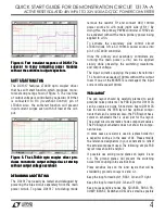
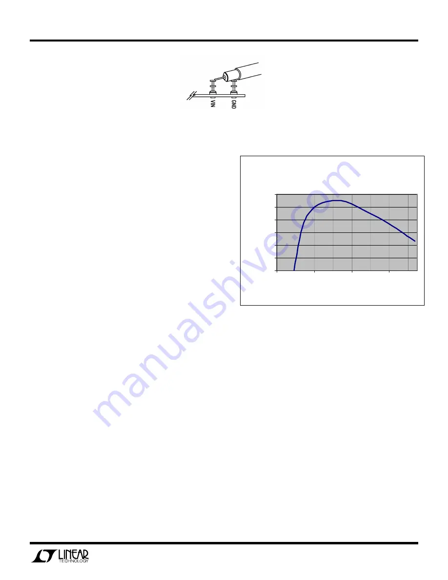
Figure 2. Scope Probe Placement for Measuring Input or Output Ri
Figure 2. Scope Probe Placement for Measuring Input or Output Ri
Figure 2. Scope Probe Placement for Measuring Input or Output Ri
Figure 2. Scope Probe Placement for Measuring Input or Output Rip
pp
pple
ple
ple
ple
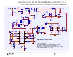
OPTIONAL PRIMARY MOS
OPTIONAL PRIMARY MOS
OPTIONAL PRIMARY MOS
OPTIONAL PRIMARY MOSFET DRIVER LTC4440
FET DRIVER LTC4440
FET DRIVER LTC4440
FET DRIVER LTC4440
The DC1317 has an optional LTC4440 MOSFET
driver U2. The LTC4440 can be used if the efficiency
is important and large MOSFET is used. The effi-
ciency gain is usually in the 0.5%-1% range when
LTC4440 is used. If required, please contact LT fac-
tory for assistance.
ACTIVE RESET CIRCUIT
ACTIVE RESET CIRCUIT
ACTIVE RESET CIRCUIT
ACTIVE RESET CIRCUIT
The Active Reset circuit on DC1317A-A demo board
consists of a small P-Channel MOSFET Q13 and
reset capacitor C25. The MOSFET Q13 is used to
connect the reset capacitor across the transformer
T1 primary winding during the reset period when
Q1 MOSFET is off. The voltage across capacitor
C25 automatically adjusts with the duty cycle to
provide complete transformer reset under all oper-
ating conditions.
Also the active reset circuit shapes the reset voltage
into a square waveform that is suitable for driving
the secondary synchronous MOSFET rectifier Q3.
Beware that the gate voltage of Q3 depends on the
reset circuit Q13 and transformer turns ratio.
The main benefit of active reset circuit in the case of
DC1317A-A demo board is high efficiency (shown
in Figure 3)and small size. To achieve such high
efficiency all of the power components were care-
fully selected. Please consult LT factory for assis-
tance if any changes to the circuit are required.
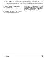
DC1317A-A (LT1952) 48Vin to 3.3V out
Efficiency
88%
89%
90%
91%
92%
93%
94%
0
10
20
30
Iout [A]
E
ff
ic
ie
n
c
y
Figure 3. High efficiency of DC1317A
Figure 3. High efficiency of DC1317A
Figure 3. High efficiency of DC1317A
Figure 3. High efficiency of DC1317A----A a
A a
A a
A alllllows
lows
lows
lows
the board to be used in thermally critical appl
the board to be used in thermally critical appl
the board to be used in thermally critical appl
the board to be used in thermally critical appli-
i-
i-
i-
cations
cations
cations
cations
OUTPUT LOAD STEP
OUTPUT LOAD STEP
OUTPUT LOAD STEP
OUTPUT LOAD STEP RESPONSE
RESPONSE
RESPONSE
RESPONSE
The load step response of DC1317A-A is very fast
even though relatively small amount of output ca-
pacitance is present (200uF ceramic and 470uF
electrolytic). This is thanks to fast error amplifier of
LT4430, optimal amount of current slope compen-
sation of LT1952, fast opto coupler and fast error
amplifier of LT1952. If higher load steps need to be
handled more output capacitance can be added in
order to keep the voltage transients at the desired
level. The load step transients are shown in Figure
4.


