
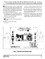


QUICK START GUIDE FOR DEMONSTRATION CIRCUIT 1317A-A
ACTIVE RESET ISOLATED 48V INPUT TO 3.3V @30A DC/DC POWER CONVERTER
4
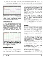
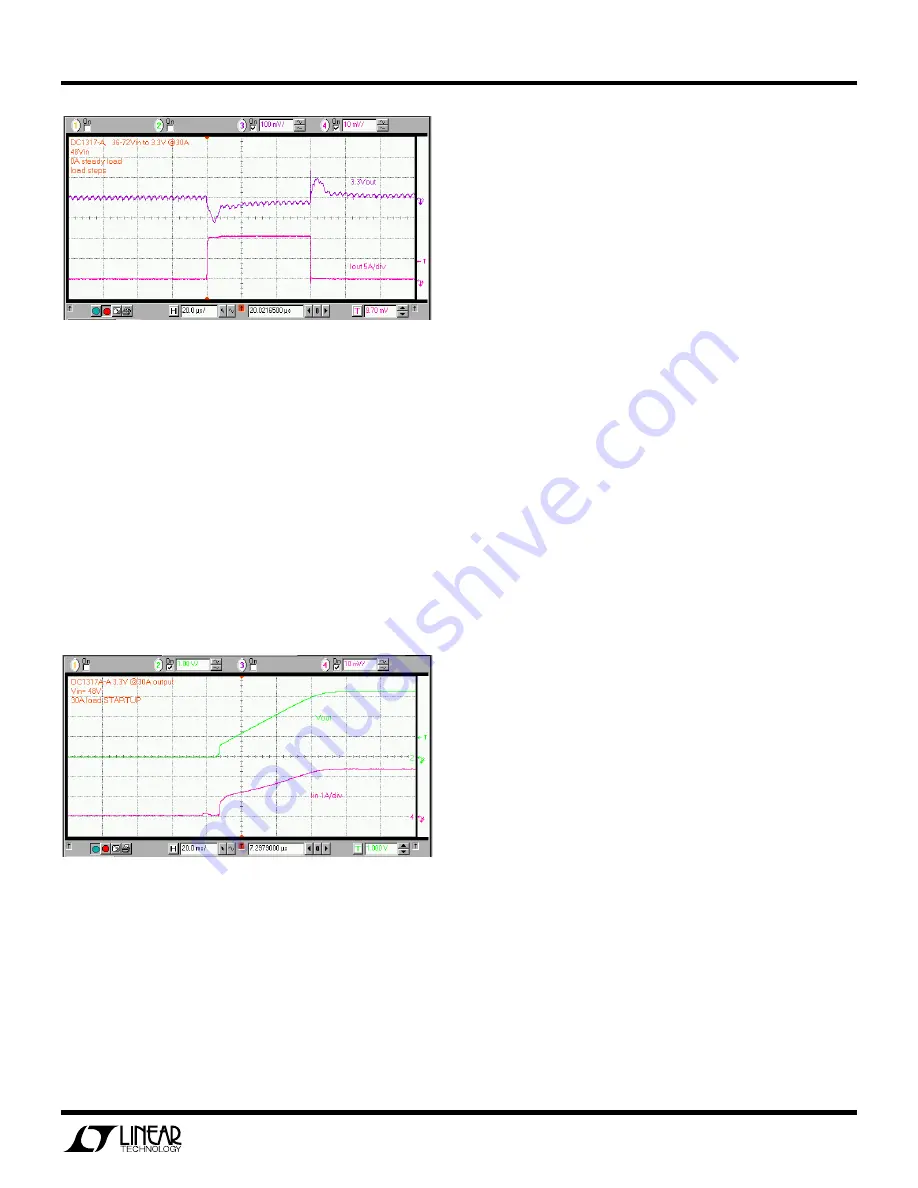
Figure 4. Fast transient response of DC1317 is
Figure 4. Fast transient response of DC1317 is
Figure 4. Fast transient response of DC1317 is
Figure 4. Fast transient response of DC1317 is
ssssu
uu
uperior to many competing power modules
perior to many competing power modules
perior to many competing power modules
perior to many competing power modules
without the additional output capac
without the additional output capac
without the additional output capac
without the additional output capaciiiitors.
tors.
tors.
tors.
SOFT START FUNCTION
SOFT START FUNCTION
SOFT START FUNCTION
SOFT START FUNCTION
The DC1317 features LT4430 opto coupler driver
that has soft start function which produces mono-
tonic startup ramp shown if Figure 5. The rise time
of output voltage is controlled by capacitor C19 that
is connected to OC (Overshoot Control) pin of
LT4430. Also, the soft-start function will prevent
input current surges even with full load at the out-
put.
Fi
Fi
Fi
Figure 5. The LT4430 opto coupler driver pr
gure 5. The LT4430 opto coupler driver pr
gure 5. The LT4430 opto coupler driver pr
gure 5. The LT4430 opto coupler driver pro-
o-
o-
o-
duces monotonic output voltage rise at startup
duces monotonic output voltage rise at startup
duces monotonic output voltage rise at startup
duces monotonic output voltage rise at startup
without ou
without ou
without ou
without outtttput voltage overshoot.
put voltage overshoot.
put voltage overshoot.
put voltage overshoot.
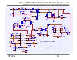
DEBUGGING AND TESTIN
DEBUGGING AND TESTIN
DEBUGGING AND TESTIN
DEBUGGING AND TESTING
G
G
G
The DC1317 can easily be tested and debugged by
powering the bias circuit separately from the main
power circuit. To place DC1317 into debug mode
remove the resistor R1 and connect 48V, 100mA
power source to +Vb node (right side of R1). By
doing this, the primary PWM controller LT1952 can
be activated without the main primary power being
applied to +Vin.
To activate the secondary side control circuit
LT4430 diode OR a 5V, 100mA power source into
pin 1 of LT4430 controller.
Once the primary and secondary controllers are
running the main power (+Vin) can be applied
slowly while observing the switching waveforms
and output voltage.
The input current supplying the power transformer
T1 should not exceeded 100mA without the output
load. If one of the MOSFETs is damaged, the input
current will exceed 100mA.
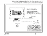
PCB LAYOUT
PCB LAYOUT
PCB LAYOUT
PCB LAYOUT
The pcb layout should be carefully planned to avoid
potential noise problems. The PCB layout for DC1317A
can be used as a guide. Since demo board DC1317A
has 8 versions the PCB layout has optional compo-
nents that can be removed. Also, the PCB layout has a
common schematic that is used just for the layout.
The actual circuit schematic shows component values.
The PCB layout schematic does not show the compo-
nent values.
In some cases, a resistor is used in a place holder for
a capacitor such as in the case of C4. Please modify
the reference designators in your schematic to reflect
the actual component used. The following simple PCB
layout rules should be helpful.
If possible use solid ground planes on layers 2 and
n-1. The ground planes will prevent the switching
noise from coupling into sensitive lines.
Place sensitive lines on the inner layers that will be
shielded by grounds on layers 2 and n-1.
Keep the loop formed by Q1, RCS1, Cin and T1 tight.
Keep the loop formed by Q2, Q3 and T1 tight.
Keep noise sensitive nodes like SD/VSEC, ROSC, FB,
COMP, ISENSE, BLANK and DELAY as small as posible


