background image

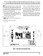
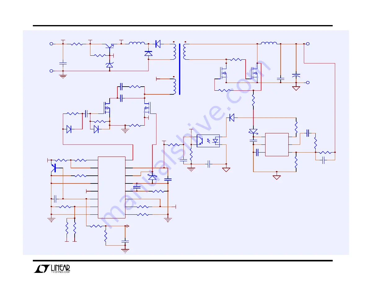
QUICK START GUIDE FOR DEMONSTRATION CIRCUIT 1317A-A 

ACTIVE RESET ISOLATED 48V INPUT TO 3.3V @30A DC/DC POWER CONVERTER 


6


Rcs1
0.015R

+Vin

R29
22K

Cu1
4.7u

R23 1.2k

R24
39K

Vu1

R15

115k

R20
174k

C10
0.1u

CS

Q1

D10

B

A

T

7

6

0

C15

2.2nF, 2kV

R28
442k

R22

13.3k

Si7430

PA0861.004

GND

8

SD

7

MaxDC

5

FB=1.23V

2

Comp

1

Rosc

3

Vr=2.5V

6

Blank

9

Delay

12

OC

11

Sync

4

Isense

10

PGND

13

Out

14

Vin

15

Sout

16

U1
LT1952-1

R33
470k

C13
.47u

SS

SS

R26
220R

R30
1.2k

R14
33K

C23
1uF

Vfb

Vfb

R13
22K

C

o

1

2

x

1

0

0

u

F

R27
470

R38
18.2K

R35
82.5k

R34
4.75k

C19
1uF

C16

0.22uF

C17
10n

CS

SS

3

Vcc

1

FB

4

Opto

6

GND

2

Comp

5

U4

LT4430

Cin
2x2.2uF

+Vin

D5
PDZ10B

Vu1

D2

BAS516

R11
82k

1

6

+Vin

R1

2.2R

R32
332k

L1

PA1671.650

Q2

HAT2165

Q3

D6
B0540W

R8
2.2R

Q12
BC856T

D3

Q10
PBSS8110

+Vb

+Vb

L2
1.5mH

U6

PS2801-1

T1

D11
BAS516

GND

+Vout

+

C

sy

s

4

7

0

u

F,

 6

.3

V

C24
47p

C9

100p

C25
10n

R49
2.2R

Q13
Si2325

D14
BAS516

R45
10k

+Vr2

+Vr2

R50
2.2R

D17
BAS516

R53
200

2, 3

4, 5

7, 8

9, 10, 11

C33
0.1u

C34
0.22uf

R54

4.7

-Vin

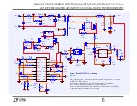
Demo Board DC1317A-A schematic

NOTE:

This schematic shows only the components required for operation of -A version
of DC1317A demo board.
All optional components of DC1317A demo board have been removed.
Also, all zero-ohm resistors have been replaced with wires.
Please consult the full DC1317A-A schematic to decide if any of the optional 
components should be included in your design.

Summary of Contents for 1317A-A

Page 1: ...t protection cir cuit that allows for continuous operation under short circuit conditions The low power dissipation under short circuit conditions insures high reliability even during short circuits The LT1952 can be synchronized to an external clock of up to 400kHz Please refer to LT1952 data sheet for design details and applications information Design files for this circuit board are avai Design...

Page 2: ... 2 2 Turn on the power at the input NOTE NOTE NOTE NOTE Make sure that the input voltage does not exceed 75V 3 3 3 3 Check for the proper output voltage Vout 3 3V If there is no output temporarily disconnect the load to make sure that the load is not set too high 4 4 4 4 Once the proper output voltage is established ad just the load within the operating range and ob serve the output voltage regula...

Page 3: ...t is suitable for driving the secondary synchronous MOSFET rectifier Q3 Beware that the gate voltage of Q3 depends on the reset circuit Q13 and transformer turns ratio The main benefit of active reset circuit in the case of DC1317A A demo board is high efficiency shown in Figure 3 and small size To achieve such high efficiency all of the power components were care fully selected Please consult LT ...

Page 4: ... tested and debugged by powering the bias circuit separately from the main power circuit To place DC1317 into debug mode remove the resistor R1 and connect 48V 100mA power source to Vb node right side of R1 By doing this the primary PWM controller LT1952 can be activated without the main primary power being applied to Vin To activate the secondary side control circuit LT4430 diode OR a 5V 100mA po...

Page 5: ...l vias for all components that connect to ground planes Do not place any traces on the layers 2 and n 1 to avoid ground planes from being compromised If the PCB layout has to be done on 2 or 4 layer PCB try to stay close to the guidelines outlined above Also maximize the ground connections between compo nents by placing the components tight together Please contact LT factory for additional assista...

Page 6: ...4 Opto 6 GND 2 Comp 5 U4 LT4430 Cin 2x2 2uF Vin D5 PDZ10B Vu1 D2 BAS516 R11 82k 1 6 Vin R1 2 2R R32 332k L1 PA1671 650 Q2 HAT2165 Q3 D6 B0540W R8 2 2R Q12 BC856T D3 Q10 PBSS8110 Vb Vb L2 1 5mH U6 PS2801 1 T1 D11 BAS516 GND Vout Csys 470uF 6 3V C24 47p C9 100p C25 10n R49 2 2R Q13 Si2325 D14 BAS516 R45 10k Vr2 Vr2 R50 2 2R D17 BAS516 R53 200 2 3 4 5 7 8 9 10 11 C33 0 1u C34 0 22uf R54 4 7 Vin Demo ...

Page 7: ...QUICK START GUIDE FOR DEMONSTRATION CIRCUIT 1317A A ACTIVE RESET ISOLATED 48V INPUT TO 3 3V 30A DC DC POWER CONVERTER 7 ...

Page 8: ...QUICK START GUIDE FOR DEMONSTRATION CIRCUIT 1317A A ACTIVE RESET ISOLATED 48V INPUT TO 3 3V 30A DC DC POWER CONVERTER 8 ...

Reviews: