background image

7

dc1369af

DEMO MANUAL DC1369A

Quick start proceDure

Internal Termination: Enables LVDS Internal Termination
•  Off (Default): Disables internal termination
•  On: Enables internal termination

Outputs: Enables Digital Outputs
•  Enabled (Default): Enables digital outputs 
•  Disabled: Disables digital outputs

Output Mode: Selects Digital Output Mode
•  Full Rate: Full rate CMOS output mode (This mode is 

not supported by the DC1369A, please use the DC1370)

•  Double LVDS (Default): Double data rate LVDS output 

mode

•  Double CMOS: Double data rate CMOS output mode 

(This mode is not supported by the DC1369A, please 

use the DC1370)

Test Pattern: Selects Digital Output Test Patterns
•  Off (Default): ADC data presented at output
•  All Out = 1: All digital outputs are 1
•  All Out = 0: All digital outputs are 0
•  Checkerboard: OF, and D13-D0 Alternate between 101 

0101 1010 0101 and 010 1010 0101 1010 on alternat-

ing samples.

•  Alternating: Digital outputs alternate between all 1’s and 

all 0’s on alternating samples.

Alternate Bit: Alternate Bit Polarity (ABP) Mode 
•  Off (Default): Disables alternate bit polarity
•  On: Enables alternate bit polarity (Before enabling ABP, 

be sure the part is in offset binary mode)

Randomizer: Enables Data Output Randomizer
•  Off (Default): Disables data output randomizer 
•  On: Enables data output randomizer

Two’s Complement: Enables Two’s Complement Mode
•  Off (Default): Selects offset binary mode
•  On: Selects two’s complement mode

Once the desired settings are selected hit OK and PScope 

will automatically update the register of the device on the 

DC1369A demo board.

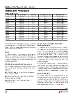
Summary of Contents for DC1369A

Page 1: ...from 5MHz to 170MHz Refer to the data sheet for proper input networks for different input frequencies Design files for this circuit board are available at http www linear com demo L LT LTC LTM Linear Technology and the Linear logo are registered trademarks and PScope and QuikEval are trademarks of Linear Technology Corporation All other trademarks are the property of their respective owners TA 25 ...

Page 2: ...to 250mA depending on the sampling rate and the A D converter supplied The DC890 data collection board is powered by the USB cableanddoesnotrequireanexternalpowersupplyunless itmustbeconnectedtothePCthroughanunpoweredhub in which case it must be supplied an external 6V to 9V on turretsG7 andG1 ortheadjacent2 1mmpowerjack Analog Input Network For optimal distortion and noise performance the RC netw...

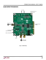
Page 3: ...igure 1 DC1369A Setup quick start procedure DC1369A F01 Analog Input 3 5V to 6V Single Ended Encode Clock Parallel Serial Programming Mode Duty Cycle Stabilizer SHDN Parallel Data Output to DC890 Jumpers Are Shown in Default Positions ...

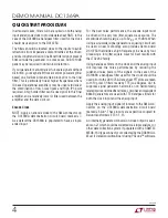
Page 4: ...r the best noise performance the encode input must be driven with a very low jitter square wave source The amplitude should be large up to 3VP P or 13dBm When using a sinusoidal signal generator a squaring circuit can be used Linear Technology also provides demo board DC1075A that divides a high frequency sine wave by four producing a low jitter square wave for best results with the LTC2262 family...

Page 5: ...by the PScope System Software provided or downloaded from the Linear Technology website at http www linear com software If a DC890 was provided follow the DC890 Quick Start Guide and the instructions below To start the data collection software if PScope exe is in stalled by default in Program Files LTC PScope double click the PScope Icon or bring up the run window under the start menu and browse t...

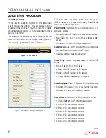
Page 6: ...p and sleep modes Normal Default Entire ADC is powered and active Nap ADC core powers down while references stay active Shutdown The entire ADC is powered down ClockInversion SelectsthepolarityoftheCLKOUTsignal Normal Default Normal CLKOUT polarity Inverted CLKOUT polarity is inverted Clock Delay Selects the phase delay of the CLKOUT signal None Default No CLKOUT delay 45 deg CLKOUT delayed by 45 ...

Page 7: ... data presented at output All Out 1 All digital outputs are 1 All Out 0 All digital outputs are 0 Checkerboard OF and D13 D0 Alternate between 101 0101 1010 0101 and 010 1010 0101 1010 on alternat ing samples Alternating Digitaloutputsalternatebetweenall1 sand all 0 s on alternating samples Alternate Bit Alternate Bit Polarity ABP Mode Off Default Disables alternate bit polarity On Enables alterna...

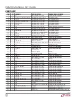
Page 8: ...1 IND 0603 56uH 5 MURATA LQP18MN56NG02D 19 3 L2 L3 L4 FERRITE BEAD 1206 MURATA BLM31PG330SN1L 20 1 L5 IND 0603 BEAD 21 1 L6 IND 0603 OPTION OPTION 22 1 P1 EDGE FINGERS ON PCB PART OF THE PCB 23 2 RN2 RN1 RES ARRAY 33Ω VISHAY CRA04SS08333R0JTD 24 2 R1 R2 RES 0402 301Ω 1 1 16W VISHAY CRCW0402301RFKED 25 3 R4 R5 R56 RES 0402 OPTION OPTION 26 1 R6 RES 0402 10kΩ 5 1 16W VISHAY CRCW040210K0JNED 27 1 R7 ...

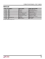
Page 9: ...ST 45 1 U3 IC FIN1108 FAIRCHILD FIN1108 46 1 U4 IC LDO Micropower Regulators LINEAR TECH LT1763CDE 1 8 47 1 U5 IC 8 BIT I 0 EXPANDER PHILIPS SEMI PCF8574TS 3 48 1 U6 IC LDO Micropower Regulators LINEAR TECH LT1763CDE 49 1 U7 IC EEPROM MICROCHIP TECH 24LC32A I ST 50 3 XJP2 XJP3 XJP4 SHUNT 2mm SAMTEC 2SN BK G 51 4 STANDOFF SNAP ON KEYSTONE_8831 See page 2 of the Schematic Diagram for U2 ...

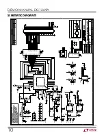
Page 10: ... C38 0 01uF C38 0 01uF L1 56uH L1 56uH C7 0 01uF C7 0 01uF 1 2 C60 0 01uF C60 0 01uF 1 2 C52 100pF C52 100pF T1 MABA 007159 000000 T1 MABA 007159 000000 C59 0 01uF C59 0 01uF 1 2 R21 100 R21 100 U1 24LC025 I ST U1 24LC025 I ST A0 1 A1 2 A2 3 A3 4 SDA 5 SCL 6 WP 7 VCC 8 R24 100K R24 100K R16 100 R16 100 R33 1K R33 1K C12 0 1uF C12 0 1uF C17 1uF C17 1uF C27 0 1uF C27 0 1uF R35 1K R35 1K R45 86 6 1 R...

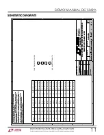
Page 11: ...HEET OF FILENAME TITLE CONTRACT NO APPROVALS DATE DRAWN CHECKED APPROVED ENGINEER DESIGNER TECHNOLOGY 1630 McCarthy Blvd Milpitas CA 95035 Phone 408 432 1900 Fax 408 434 0507 3 1 DC1369A 05 22 12 06 00 33 2 2 SCH LTC2261CUJ HIGH SPEED LOW POWER 1369A 3 DSN NONE MI 10 31 07 125MSPS ADC FAMILY LVDS Customer Notice Linear Technology has made a best effort to design a circuit that meets customer suppl...

Page 12: ...LUDING ANY WARRANTY OF MERCHANTABILITY OR FITNESS FOR ANY PARTICULAR PURPOSE EXCEPT TO THE EXTENT OF THIS INDEMNITY NEITHER PARTY SHALL BE LIABLE TO THE OTHER FOR ANY INDIRECT SPECIAL INCIDENTAL OR CONSEQUENTIAL DAMAGES The user assumes all responsibility and liability for proper and safe handling of the goods Further the user releases LTC from all claims arising from the handling or use of the go...

Page 13: ...istributor Click to View Pricing Inventory Delivery Lifecycle Information Analog Devices Inc DC1369A C DC1369A D DC1369A J DC1369A N DC1369A F DC1369A G DC1369A L DC1369A K DC1369A I DC1369A M DC1369A A DC1369A H DC1369A B DC1369A E ...

Reviews: