background image

1

dc1668abf

DEMO MANUAL DC1668A-B

DESCRIPTION

LTM4627EV High Efficiency 

40A PolyPhase Step-Down  

Power Supply 

BOARD PHOTO

Demonstration circuit 1668A-B is a PolyPhase

®

 power sup-

ply featuring three LTM

®

4627 high efficiency synchronous 

buck µModule

®

 regulators. The DC1668A-B input voltage 

range is between 4.5V to 20V with a jumper programmable 

output voltage from 0.6V to 3.3V. The demo circuit can 

deliver up to 40A of load with excellent current sharing.  

Current derating may be necessary under certain operat-

ing conditions. 
The LTM4627 can be synchronized to an external clock be-

tween 250kHz to 770kHz. The default switching frequency 

for the DC1668A-B is set to 500kHz through the onboard 

LTC6902 clock generator. The external clock interleaves 

the paralleled phases to minimize input and output ripple. 
DC1668A-B demonstrates that paralleling LTM4627 mod-

ules is easy and reliable. These features and the availability 

of the LTM4627 in a compact thermally enhanced 15mm ×  

15mm × 4.32mm LGA package make the circuit ideal for 

use in high density point of load regulation applications. 
Design files for this circuit board are available at  

http://www.linear.com/demo

L

, LT, LTC, LTM, Linear Technology, PolyPhase, µModule and the Linear logo are registered 

trademarks of Linear Technology Corporation. All other trademarks are the property of their 

respective owners.

Summary of Contents for DC1668A-B

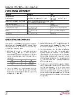
Page 1: ...e tween250kHzto770kHz Thedefaultswitchingfrequency for the DC1668A B is set to 500kHz through the onboard LTC6902 clock generator The external clock interleaves the paralleled phases to minimize input and output ripple DC1668A B demonstrates that paralleling LTM4627 mod ulesiseasyandreliable Thesefeaturesandtheavailability oftheLTM4627inacompactthermallyenhanced15mm 15mm 4 32mm LGA package make th...

Page 2: ... Place jumpers in the following positions for a typical 1 8VOUT application JP2 JP7 JP6 VOUT Select RUN TRACK SS 1 8V OFF SOFT START 2 Turn on the power at the input Increase VIN to 12V Do not hot plug the input supply or apply more than the rated maximum voltage of 20V to the board or the modules may be damaged 3 Set the RUN pin jumper JP7 to the ON position The output voltage should be regulated...

Page 3: ...3 dc1668abf DEMO MANUAL DC1668A B QUICK START PROCEDURE Figure 1 Test Setup of DC1668A B V A V A VIN BNC CABLE TO OSCILLOSCOPE TERMINATE INTO 50Ω LOAD 1668ab F01 ...

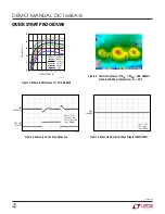
Page 4: ... 8VOUT 40A 500kHz No Forced Airflow Convection TA 29 C Figure 5 Measured Output Voltage Ripple 20MHz BW LOAD CURRENT A 0 EFFICIENCY 25 20 15 1668ab F02 95 90 10 5 40 35 30 85 80 75 70 3 3VOUT 2 5VOUT 1 8VOUT 1 5VOUT 1 2VOUT 1VOUT 1668ab F04 20A DIV 100mV DIV VOUT IOUT STEP VOUT 1 8V IOUT DC 20A IOUT STEP 20A fSW 500kHz 1668ab F05 50mV DIV VOUT VOUT 1 8V IOUT 40A fSW 500kHz ...

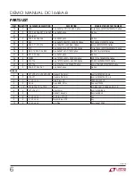
Page 5: ... 10W Vishay CRCW060330K1FKEA 19 1 R14 Res 0603 20k 1 1 10W Vishay CRCW060320K0FKEA 20 1 R29 Res 0603 133k 1 1 10W Vishay CRCW0603133KFKEA 21 3 U1 U2 U3 IC µModule Regulator Linear Technology LTM4627EV Additional Demo Board Circuit Components 1 2 C14 C38 Cap 0603 0 1µF 20 16V X7R Taiyo Yuden EMK107BJ104MA T 2 1 C16 Cap 0603 1µF 20 10V X5R Taiyo Yuden LMK107BJ105MA T 3 1 C60 Cap 0603 1000pF 10 50V N...

Page 6: ...ption 27 0 R21 R22 R36 Res 0603 Option Option 28 0 CIN22 Cap 1210 22µF 20 25V X5R Option AVX 12103D226MAT2A Option 29 0 COUT13 Cap 1812 100µF 20 6 3V X5R Option TDK C4532X5R0J107MZ Option 30 0 COUT25 Cap 470µF 20 4V POSCAP Option Sanyo POSCAP 4TPF470ML Option 31 0 R26 R27 C54 C67 Cap 0603 Option Option Hardware 1 6 JP1 JP2 JP3 JP4 JP5 JP8 Header 2 Pin 2mm Samtec TMM 102 02 L S 2 2 JP6 JP7 Header 3...

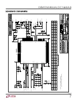
Page 7: ...P14 C61 C61 COUT1 100uF 6 3V COUT1 100uF 6 3V TP2 TP2 R8 0 R8 0 R17 0 015 1 R17 0 015 1 C18 OPT C18 OPT COUT24 OPT COUT24 OPT TP4 TP4 R21 OPT R21 OPT JP5 JP5 TP1 TP1 JP1 JP1 R14 1 R14 1 Q14 SUD50N03 10CP Q14 SUD50N03 10CP 1 2 3 J5 J5 1 2 3 4 5 R2 1 R2 1 R19 10 R19 10 TP6 TP6 JP8 JP8 CIN14 OPT 25V CIN14 OPT 25V TP5 TP5 C69 OPT C69 OPT 1 2 R13 OPT R13 OPT COUT2 OPT COUT2 OPT J1 J1 C55 OPT C55 OPT R1...

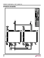
Page 8: ...D G4 PGND G5 PGND G6 PGND G7 PGND G8 PGND G9 PGND H1 PGND H2 PGND H3 PGND H4 PGND H5 PGND H6 PGND H7 PGND H8 PGND H9 SGND H11 SGND H12 PGND C9 PGND C7 PGND B9 PGND B7 PGND D8 PGND E9 PGOOD F11 PGOOD G12 MTP8 D12 MTP7 D11 MTP6 D10 MTP5 C12 MTP4 C11 MTP3 C10 MTP2 B11 EXTVCC E12 MTP1 A12 C52 C52 C64 1nF C64 1nF C76 OPT C76 OPT COUT5 100uF COUT5 100uF COUT10 OPT COUT10 OPT COUT6 OPT COUT6 OPT R23 OPT ...

Page 9: ...LTM4627EV U4 LTM4627EV SGND G11 FSET B12 VOUT_LCL L12 COMP A11 VFB F12 RUN A10 TRACK SS A9 PLLIN A8 INTVCC A7 VOSNS J12 VOSNS M12 DIFF_VOUT K12 INTVCC D9 VIN A1 VIN A2 VIN A3 VIN A4 VIN A5 VIN A6 VIN B1 VIN B2 VIN B3 VIN B4 VIN B5 VIN B6 VIN C1 VIN C2 VIN C3 VIN C4 VIN C5 VIN C6 VOUT J1 VOUT J2 VOUT J3 VOUT J4 VOUT J5 VOUT J6 VOUT J7 VOUT J8 VOUT J9 VOUT J10 VOUT K1 VOUT K2 VOUT K3 VOUT K4 VOUT K5...

Page 10: ...NCLUDING ANY WARRANTY OF MERCHANTABILITY OR FITNESS FOR ANY PARTICULAR PURPOSE EXCEPT TO THE EXTENT OF THIS INDEMNITY NEITHER PARTY SHALL BE LIABLE TO THE OTHER FOR ANY INDIRECT SPECIAL INCIDENTAL OR CONSEQUENTIAL DAMAGES The user assumes all responsibility and liability for proper and safe handling of the goods Further the user releases LTC from all claims arising from the handling or use of the ...

Reviews: