background image

4

dc1925af

DEMO MANUAL DC1925A

DC1925A SETUP

Data Collection
For SINAD, THD or SNR testing a low noise, low distortion 

differential output sine generator such as the Stanford 

Research DS360 should be used. A low jitter RF oscillator 

such as the Rohde & Schwarz SMB100A or DC1216A-C 

is used as the clock source. 
This  demo  board  is  tested  in  house  by  attempting  to 

duplicate the FFT plot shown in the typical performance 

characteristics of the LTC2378-20 data sheet. This involves 

using an 80MHz clock source, along with a differential 

output  sinusoidal  generator  at  a  frequency  of 2.0kHz. 

The input signal level is approximately –1dBfs. The input 

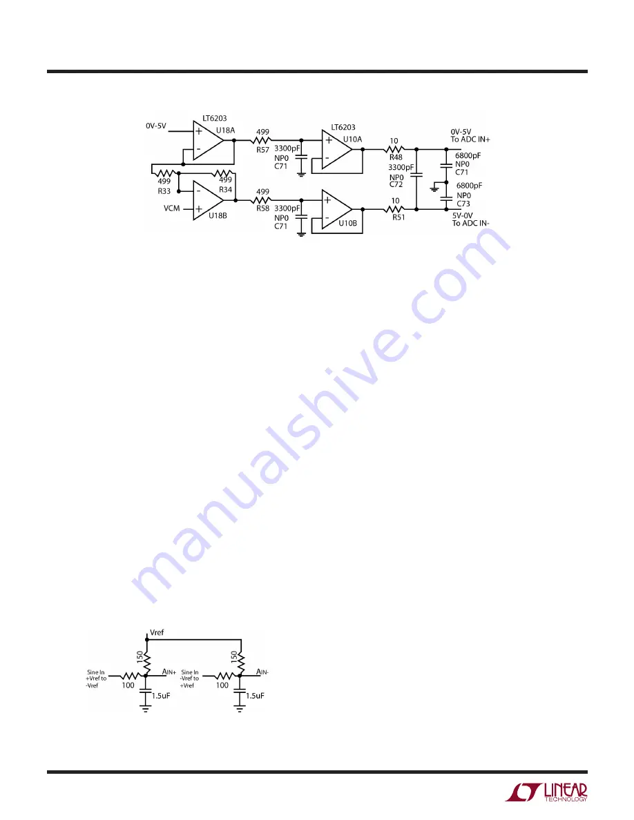
is level shifted and filtered with the circuit shown in Fig-

ure 4. A typical FFT obtained with DC1925A is shown in 

Figure 5. Note that to calculate the real SNR, the signal level  

(F1 amplitude = –0.998dB) has to be added back to the 

SNR that PScope displays. With the example shown in Fig-

ure 5 this means that the actual SNR would be 103.668dB 

instead of the 102.67dB that PScope displays. Taking the 

RMS sum of the recalculated SNR and the THD yields a 

SINAD of 103.62dB which is fairly close to the typical 

number for this ADC.

Figure 3. Single-Ended-to-Differential Driver

There are a number of scenarios that can produce mislead-

ing results when evaluating an ADC. One that is common 

is feeding the converter with a frequency, that is a sub-

multiple of the sample rate, and which will only exercise 

a small subset of the possible output codes. The proper 

method is to pick an M/N frequency for the input sine wave 

frequency. N is the number of samples in the FFT. M is 

a prime number between one and N/2. Multiply M/N by 

the sample rate to obtain the input sine wave frequency. 

Another scenario that can yield poor results is if you do 

not have a sine generator capable of ppm frequency ac-

curacy or if it cannot be locked to the clock frequency. You 

can use an FFT with windowing to reduce the “leakage” or 

spreading of the fundamental, to get a close approxima-

tion of the ADC performance. If windowing is required, 

the Blackman-Harris 92dB window is recommended. If an 

amplifier or clock source with poor phase noise is used, 

windowing will not improve the SNR.

Layout
As with any high performance ADC, this part is sensitive 

to layout. The area immediately surrounding the ADC on 

the DC1925A should be used as a guideline for placement, 

and routing of the various components associated with the 

ADC. Here are some things to remember when laying out a 

board for the LTC2378-20. A ground plane is necessary to 

obtain maximum performance. Keep bypass capacitors as 

close to supply pins as possible. Use low impedance returns 

directly to the ground plane for each bypass capacitor. 

Use of a symmetrical layout around the analog inputs will 

minimize the effects of parasitic elements. Shield analog 

Figure 4. Differential Level Shifter

Summary of Contents for DC1925A Series

Page 1: ...ing on the information therein All referenced brands product names service names and trademarks are the property of their respective owners 00000005981LF 000 EOS Power Buy Now We have 45 000 LP502030 PCM NTC LD A02554 EEMB Lithium Battery Rectangular 3 7V 250mAh Rechargeable in stock now Starting at 0 034 This EEMB part is fully warrantied and traceable 1 855 837 4225 Give us a call International ...

Page 2: ...LTC2378 20 in conjunction with the DC590 QuikEval and DC890 PScope data collection boards Use the DC590 to demonstrate DC performance such as L LT LTC LTM Linear Technology and the Linear logo are registered trademarks and QuikEval and PScope are trademarks of Linear Technology Corporation All other trademarks are the property of their respective owners BOARD PHOTO Figure 1 DC1925A Connection Diag...

Page 3: ...te that J1 has a 50Ω termination resistor to ground Run the PScope software PScope exe version K73 or later supplied with the DC890 or download it from www linear com software Complete software documentation is available from the Help menu Updates can be downloaded from the Tools menu Check for updates periodically as new features may be added The PScope software should recognize the DC1925A and c...

Page 4: ...ssing is desired Alternatively the data can be fed directly into an application circuit Use Pin 50 of P1 to latch the data The data can be latched using either edge of this signal The data output signal levels at P1 can also be changed to 0V to 3 3V if the application circuit requires a higher voltage This is accomplished by moving VCCIO JP3 to the 3 3V position Reference The default reference is ...

Page 5: ...on is feeding the converter with a frequency that is a sub multiple of the sample rate and which will only exercise a small subset of the possible output codes The proper methodistopickanM Nfrequencyfortheinputsinewave frequency N is the number of samples in the FFT M is a prime number between one and N 2 Multiply M N by the sample rate to obtain the input sine wave frequency Another scenario that...

Page 6: ...8 20 component selection is important so as to not degrade performance Resistors should have low values to minimize noise and distortion Metal film resistors are recommended to reduce distortion caused by self heating Because of their low voltage coefficients to further reduce distortion NPO or silver mica capacitors should be used Any buffer used to drive the LTC2378 20 should have low distortion...

Page 7: ...6 dc1925af DEMO MANUAL DC1925A DC1925A SETUP Figure 6 QuikEval Screen Shot ...

Page 8: ...differential mode is enabled and the inputs are AC coupled VREF 2 is the default setting JP5 V Selects 3 6V or ground for V The default set ting is 3 6V Setting V to ground is useful for evaluating single supply operation of the buffer when operating the ADC with Digital Gain Compression turned on JP6 FS selects whether the Digital Gain Compression is on or off In the VREF position Digital Gain Co...

Page 9: ...VX 06036D475MAT2A 17 7 E1 E2 E3 E4 E5 E9 E10 TEST POINT TURRET 0 061 MILL MAX 2308 2 00 80 00 00 07 0 18 3 E6 E7 E8 TESTPOINT TURRET 0 094 PBF MILL MAX 2501 2 00 80 00 00 07 0 19 8 JP1 JP8 HEADER 3 PIN SINGLE ROW 0 100 SAMTEC TSW 103 07 L S 20 3 J1 J2 J4 CONNECTOR BNC CONNEX 112404 21 1 J3 CONN HEADER 14 POS 2MM VERT GOLD MOLEX 87831 1420 22 1 J5 HEADER 2X5 0 100 SAMTEC TSW 105 07 L D 23 4 MH1 MH2...

Page 10: ... IC SERIAL EEPROM TSSOP MICROCHIP 24LC024 I ST 52 2 U8 U9 IC UHS INVERTER SC70 5 FAIRCHILD NC7SZ04P5X 53 2 U10 U18 IC DUAL OP AMP MS8 LINEAR TECH LT6203CMS8 PBF 54 1 U11 IC MAX II CPLD TQFP100 ALTERA EPM240GT100C5N 55 1 U12 IC MICROPOWER REGULATOR SO 8 LINEAR TECH LT1763CS8 1 8 PBF 56 2 U13 U16 IC MICROPOWER REGULATOR SO 8 LINEAR TECH LT1763CS8 PBF 57 1 U14 IC MICROPOWER REGULATOR SO 8 LINEAR TECH...

Page 11: ...10 dc1925af DEMO MANUAL DC1925A SCHEMATIC DIAGRAM ...

Page 12: ...logy Corporation is believed to be accurate and reliable However noresponsibilityisassumedforitsuse LinearTechnologyCorporationmakesnorepresenta tion that the interconnection of its circuits as described herein will not infringe on existing patent rights SCHEMATIC DIAGRAM ...

Page 13: ...UDING ANY WARRANTY OF MERCHANTABILITY OR FITNESS FOR ANY PARTICULAR PURPOSE EXCEPT TO THE EXTENT OF THIS INDEMNITY NEITHER PARTY SHALL BE LIABLE TO THE OTHER FOR ANY INDIRECT SPECIAL INCIDENTAL OR CONSEQUENTIAL DAMAGES The user assumes all responsibility and liability for proper and safe handling of the goods Further the user releases LTC from all claims arising from the handling or use of the goo...

Reviews: