background image

LT8302

15

8302fb

For more information 

www.linear.com/LT8302

applicaTions inForMaTion

Turns Ratio

Note that when choosing an R

FB

/R

REF

 resistor ratio to set 

output voltage, the user has relative freedom in selecting 

a transformer turns ratio to suit a given application. In 

contrast, the use of simple ratios of small integers, e.g., 

3:1, 2:1, 1:1, etc., provides more freedom in settling total 

turns and mutual inductance.
Typically, choose the transformer turns ratio to maximize 

available  output  power.  For  low  output  voltages (3.3V 

or 5V), a N:1 turns ratio can be used with multiple pri-

mary windings relative to the secondary to maximize the 

transformer’s current gain (and output power). However, 

remember that the SW pin sees a voltage that is equal 

to  the  maximum  input  supply  voltage  plus  the  output 

voltage multiplied by the turns ratio. In addition, leakage 

inductance will cause a voltage spike (V

LEAKAGE

) on top of 

this reflected voltage. This total quantity needs to remain 

below the 65V absolute maximum rating of the SW pin to 

prevent breakdown of the internal power switch. Together 

these conditions place an upper limit on the turns ratio, 

N

PS

,  for  a  given  application.  Choose  a  turns  ratio  low 

enough to ensure


N

PS

<

65V – V

IN(MAX)

– V

LEAKAGE

V

OUT

+

V

F

For larger N:1 values, choose a transformer with a larger 

physical  size  to  deliver  additional  current.  In  addition, 

choose a large enough inductance value to ensure that 

the switch-off time is long enough to accurately sample 

the output voltage.
For lower output power levels, choose a 1:1 or 1:N trans-

former for the absolute smallest transformer size. A 1:N 

transformer  will  minimize  the  magnetizing  inductance 

(and minimize size), but will also limit the available output 

power. A higher 1:N turns ratio makes it possible to have 

very high output voltages without exceeding the breakdown 

voltage of the internal power switch.

The turns ratio is an important element in the isolated 

feedback scheme, and directly affects the output voltage 

accuracy. Make sure the transformer manufacturer speci-

fies turns ratio accuracy within ±1%.

Saturation Current

The current in the transformer windings should not exceed 

its rated saturation current. Energy injected once the core is 

saturated will not be transferred to the secondary and will 

instead be dissipated in the core. When designing custom 

transformers to be used with the LT8302, the saturation 

current  should  always  be  specified  by  the  transformer 

manufacturers.

Winding Resistance

Resistance in either the primary or secondary windings 

will reduce overall power efficiency. Good output voltage 

regulation will be maintained independent of winding re-

sistance due to the boundary/discontinuous conduction 

mode operation of the LT8302.

Leakage Inductance and Snubbers

Transformer leakage inductance on either the primary or 

secondary causes a voltage spike to appear on the primary 

after the power switch turns off. This spike is increasingly 

prominent at higher load currents where more stored en-

ergy must be dissipated. It is very important to minimize 

transformer leakage inductance.
When designing an application, adequate margin should 

be kept for the worst-case leakage voltage spikes even 

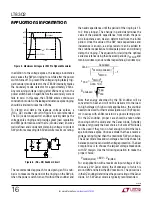
under overload conditions. In most cases shown in Fig-

ure 5, the reflected output voltage on the primary plus V

IN


should be kept below 50V. This leaves at least 15V margin 

for the leakage spike across line and load conditions. A 

larger voltage margin will be required for poorly wound 

transformers or for excessive leakage inductance.

Summary of Contents for LT8302

Page 1: ...32VIN 5VOUT Isolated Flyback Converter Applications n 2 8V to 42V Input Voltage Range n 3 6A 65V Internal DMOS Power Switch n Low Quiescent Current 106µA in Sleep Mode 380µA in Active Mode n Quasi Resonant Boundary Mode Operation at Heavy Load n Low Ripple Burst Mode Operation at Light Load n Minimum Load 0 5 Typ of Full Output n No Transformer Third Winding or Opto Isolator Required for Output Vo...

Page 2: ...EAD FREE FINISH TAPE AND REEL PART MARKING PACKAGE DESCRIPTION TEMPERATURE RANGE LT8302ES8E PBF LT8302ES8E TRPBF 8302 8 Lead Plastic SO 40 C to 125 C LT8302IS8E PBF LT8302IS8E TRPBF 8302 8 Lead Plastic SO 40 C to 125 C LT8302HS8E PBF LT8302HS8E TRPBF 8302 8 Lead Plastic SO 40 C to 150 C LT8302MPS8E PBF LT8302MPS8E TRPBF 8302 8 Lead Plastic SO 55 C to 150 C Consult LTC Marketing for parts specified...

Page 3: ...itch Current Limit 0 78 0 87 0 96 A RDS ON Switch On Resistance ISW 1 5A 80 mΩ ILKG Switch Leakage Current VSW 65V 0 1 0 5 µA tSS Soft Start Timer 11 ms Note 1 Stresses beyond those listed under Absolute Maximum Ratings may cause permanent damage to the device Exposure to any Absolute Maximum Rating condition for extended periods may affect device reliability and lifetime Note 2 The SW pin is rate...

Page 4: ... 50mV DIV 2µs DIV FRONT PAGE APPLICATION VIN 12V IOUT 2A 8302 G04 VSW 20V DIV VOUT 50mV DIV 2µs DIV FRONT PAGE APPLICATION VIN 12V IOUT 0 5A 8302 G05 VSW 20V DIV VOUT 50mV DIV 20µs DIV FRONT PAGE APPLICATION VIN 12V IOUT 10mA 8302 G06 VIN V 0 I Q µA 6 8 10 40 8302 G07 4 2 0 10 20 30 50 TJ 150 C TJ 25 C TJ 55 C VIN V 0 80 I Q µA 90 100 110 120 130 140 10 20 30 40 8302 G08 50 TJ 150 C TJ 55 C TJ 25 ...

Page 5: ...VCC V 2 85 2 90 2 95 3 00 0 50 100 150 8302 G12 3 05 3 10 25 25 75 125 IINTVCC 0mA IINTVCC 10mA VIN V 5 V INTVCC V 2 95 3 00 3 05 35 40 20 25 30 8302 G13 2 90 2 85 10 15 45 2 80 3 10 IINTVCC 0mA IINTVCC 10mA TEMPERATURE C 50 2 2 V INTVCC V 2 3 2 4 2 5 2 6 0 50 100 150 8302 G14 2 7 2 8 25 25 75 125 FALLING RISING TEMPERATURE C 50 VOLTAGE mV 0 20 150 8302 G15 20 40 0 50 100 25 25 75 125 40 10 10 30 ...

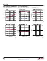
Page 6: ...0 160 200 25 75 150 8302 G19 80 40 0 25 0 50 100 125 TEMPERATURE C 50 I SW A 3 4 5 25 75 150 8302 G20 2 1 0 25 0 50 100 125 MAXIMUM CURRENT LIMIT MINIMUM CURRENT LIMIT TEMPERATURE C 50 FREQUENCY kHz 300 400 500 25 75 150 8302 G21 200 100 0 25 0 50 100 125 TEMPERATURE C 50 FREQUENCY kHz 12 16 20 25 75 150 8302 G22 8 4 0 25 0 50 100 125 TEMPERATURE C 50 0 TIME ns 100 200 300 400 25 0 25 50 8302 G23 ...

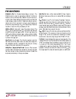
Page 7: ...posed Pad Pin 9 Ground The exposed pad provides both electrical contact to ground and good thermal contact to the printed circuit board Solder the exposed pad directly to the ground plane SW Pin 5 Drain of the Internal DMOS Power Switch Minimize trace area at this pin to reduce EMI and voltage spikes RFB Pin 6 Input Pin for External Feedback Resistor Connectaresistorfromthispintothetransformerprim...

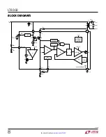
Page 8: ...VCC VIN T1 N 1 A2 RSENSE A3 TC 8302 BD RREF RREF REN2 REN1 RTC RFB gm 1 214V 1V M4 OSCILLATOR LDO BOUNDARY DETECTOR START UP REFERENCE CONTROL PTAT VOLTAGE R M1 GND 4 EXPOSED PAD PIN 9 Q S M2 VIN VIN CIN 6 RFB 5 SW L1A L1B COUT DOUT VOUT VOUT M3 25µA INTVCC 1 EN UVLO CINTVCC 2 5µA 1 4 7 A1 ...

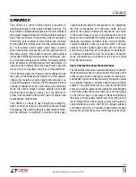
Page 9: ...ted fly back converter housed in a thermally enhanced 8 lead SO package The output voltage is programmed with two external resistors An optional TC resistor provides easy output diode temperature compensation By integrating the loop compensation and soft start inside the part reduces the number of external components As shown in the Block Diagram many of the blocks are similar to those found in tr...

Page 10: ...lamp the part starts to delay the switch turn on and operates in discontinuous conduction mode Low Ripple Burst Mode Operation Unlike traditional flyback converters the LT8302 has to turn on and off at least for a minimum amount of time andwithaminimumfrequencytoallowaccuratesampling of the output voltage The inherent minimum switch cur rent limit and minimum switch off time are necessary to guara...

Page 11: ...tage at the RREF pin to be nearly equal to the internal referencevoltageVREF Theresultingrelationshipbetween VFLBK and VREF can be expressed as VFLBK RFB RREF VREF or VFLBK VREF RFB RREF VREF Internal reference voltage 1 00V Combination with the previous VFLBK equation yields an equation for VOUT in terms of the RFB and RREF resistors transformer turns ratio and diode forward voltage VOUT VREF RFB...

Page 12: ...s to yield nominal RFB RREF ratios First build and power up the application with the starting RREF RFB values no RTC resistor yet and other compo nents connected and measure the regulated output volt age VOUT MEAS The new RFB value can be adjusted to RFB NEW VOUT VOUT MEAS RFB Second with a new RFB resistor value selected the output diode temperature coefficient in the application can be tested to...

Page 13: ...ur ing the switch off time 15V of margin is left for leakage inductance voltage spike To achieve this power level at a given input a winding ratio value must be calculated to stress the switch to 50V resulting in some odd ratio values The curves below the maximum output power curve are examples of common winding ratio values and the amount of output power at given input voltages One design example...

Page 14: ...ose a transformer with its primary mag netizing inductance about 40 to 60 larger than the minimum values calculated above A transformer with much larger inductance will have a bigger physical size and may cause instability at light load Selecting a Transformer Transformer specification and design is perhaps the most criticalpartofsuccessfullyapplyingtheLT8302 Inaddition to the usual list of guidel...

Page 15: ...g inductance and minimize size but will also limit the available output power A higher 1 N turns ratio makes it possible to have veryhighoutputvoltageswithoutexceedingthebreakdown voltage of the internal power switch The turns ratio is an important element in the isolated feedback scheme and directly affects the output voltage accuracy Make sure the transformer manufacturer speci fies turns ratio ...

Page 16: ...e is known a series resistor can be added to the snubber capacitance to dissipate power and critically damp the ringing The equation for deriving the optimal seriesresistanceusingtheobservedperiods tPERIOD and tPERIOD SNUBBED andsnubbercapacitance CSNUBBER is CPAR CSNUBBER tPERIOD SNUBBED tPERIOD 2 1 LPAR tPERIOD 2 CPAR 4π2 RSNUBBER LPAR CPAR Note that energy absorbed by the RC snubber will be con...

Page 17: ...imum load requirement which can be approximately estimated as ILOAD MIN LP 2 RI ISW MIN fMIN 2 VOUT LPRI Transformer primary inductance ISW MIN Minimumswitchcurrentlimit 0 96A MAX fMIN Minimum switching frequency 12 7kHz MAX TheLT8302typicallyneedslessthan0 5 ofitsfulloutput power as minimum load Alternatively a Zener diode with its breakdown of 10 higher than the output voltage can serve as a min...

Page 18: ...io NPS VSW MAX at VIN MAX V IOUT MAX at VIN MIN A DUTY CYCLE 1 1 37 3 0 92 14 40 2 1 42 6 1 31 25 57 3 1 47 9 1 53 33 67 Clearly only NPS 3 can meet the 1 5A output current requirement so NPS 3 is chosen as the turns ratio in this example Step 2 Determine the primary inductance Primary inductance for the transformer must be set above a minimum value to satisfy the minimum switch off and switch on ...

Page 19: ...sen Step 4 Choose the output capacitor The output capacitor should be chosen to minimize the outputvoltageripplewhileconsideringtheincreaseinsize and cost of a larger capacitor Use the following equation to calculate the output capacitance COUT LPRI ISW 2 2 VOUT ΔVOUT Example Design for output voltage ripple less than 1 of VOUT i e 100mV COUT 9µH 4 5A 2 2 5V 0 1V 182µF Remember ceramic capacitors ...

Page 20: ...nput voltage across the operating tempera ture range Calculate the temperature coefficient of VF δVF δT VOUT T1 VOUT T2 T1 T2 RTC 3 35mV C δVF δT RFB NPS Example δVF δT 5 189V 5 041V 100 C 0 C 1 48mV C RTC 3 35mV C 1 48mV C 154 3 115k Step 9 Select the EN UVLO resistors Determinetheamountofhysteresisrequiredandcalculate R1 resistor value VIN HYS 2 5µA R1 Example Choose 2V of hysteresis R1 806k Det...

Page 21: ...RRENT mA 0 11 2 OUTPUT VOLTAGE V 11 4 11 6 11 8 12 0 12 2 12 4 200 400 600 800 1000 1200 8302 TA02c VIN 12V VIN 24V VIN LT8302 SW 9µH VIN 8V TO 32V T1 1 1 9µH RFB RREF C3 470pF Z1 D1 D2 C1 10µF C2 1µF C4 47µF VOUT 12V 5mA TO 0 8A VIN 12V 5mA TO 1 1A VIN 24V VOUT R3 39Ω R4 121k R6 OPEN R2 232k R1 806k R5 10k D1 DIODES DFLS1100 D2 DIODES PDS540 T1 WURTH 750313443 Z1 CENTRAL CMZ5934B 8302 TA02a TC EN...

Page 22: ...µH D3 C5 22µF VOUT2 12V 5mA TO 0 4A VIN 12V 5mA TO 0 55A VIN 24V VOUT2 EN UVLO GND INTVCC VIN LT8302 SW 9µH VIN 8V TO 36V T1 1 2 36µH RFB RREF C3 470pF Z1 D1 D2 C1 10µF C2 1µF C4 10µF VOUT 24V 2 5mA TO 0 4A VIN 12V 2 5mA TO 0 55A VIN 24V VOUT R3 39Ω R4 121k R6 OPEN R2 232k R1 806k R5 10k D1 DIODES DFLS1100 D2 DIODES SBR2U150SA T1 WURTH 750313445 Z1 CENTRAL CMZ5934B 8302 TA05 TC EN UVLO GND INTVCC ...

Page 23: ...Buck Boost Converter 18V to 42VIN 12VOUT Negative Buck Converter Efficiency vs Load Current Efficiency vs Load Current Efficiency vs Load Current VIN SW LT8302 L1 12µH D1 Z1 GND RFB RREF EN UVLO C3 47µF D1 DIODES PMEG6030EP L1 WÜRTH 744770112 Z1 CENTRAL CMHZ5243B C2 1µF VIN 4V TO 42V C1 10µF R5 10k 8302 TA08a VOUT 12V 0 45A VIN 5V 12V 0 8A VIN 12V 12V 1 1A VIN 24V 12V 1 3A VIN 42V R4 118k INTVCC L...

Page 24: ...3 988 NOTE 3 8 7 005 0 13 MAX 6 5 189 197 4 801 5 004 NOTE 3 228 244 5 791 6 197 160 005 4 06 0 127 118 2 99 REF RECOMMENDED SOLDER PAD LAYOUT 045 005 1 143 0 127 050 1 27 BSC INCHES MILLIMETERS NOTE 1 DIMENSIONS IN 2 DRAWING NOT TO SCALE 3 THESE DIMENSIONS DO NOT INCLUDE MOLD FLASH OR PROTRUSIONS MOLD FLASH OR PROTRUSIONS SHALL NOT EXCEED 010 0 254mm 4 STANDARD LEAD STANDOFF IS 4mils TO 10mils DA...

Page 25: ...lityisassumedforitsuse LinearTechnologyCorporationmakesnorepresenta tion that the interconnection of its circuits as described herein will not infringe on existing patent rights Revision History REV DATE DESCRIPTION PAGE NUMBER A 11 14 Modified IQ and IHYS Conditions Modified LPRI Equation Modified Schematic Updated Related Parts 3 14 23 26 B 11 15 Revised Package Drawing 24 ...

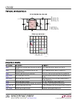
Page 26: ...r Isolated Flyback Converter with 65V 1 2A Switch Low IQ Monolithic No Opto Flyback 5 Lead TSOT 23 LT8300 100VIN Micropower Isolated Flyback Converter with 150V 260mA Switch Low IQ Monolithic No Opto Flyback 5 Lead TSOT 23 LT8309 Secondary Side Synchronous Rectifier Driver 4 5V VCC 40V Fast Turn On and Turn Off 5 Lead TSOT 23 LT3573 LT3574 LT3575 40V Isolated Flyback Converters Monolithic No Opto ...

Reviews: