


Chapter 10 Maintenance
XBC E-Type Main Unit
10-14
Ver. 1
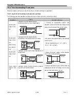
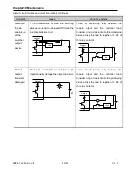
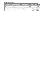
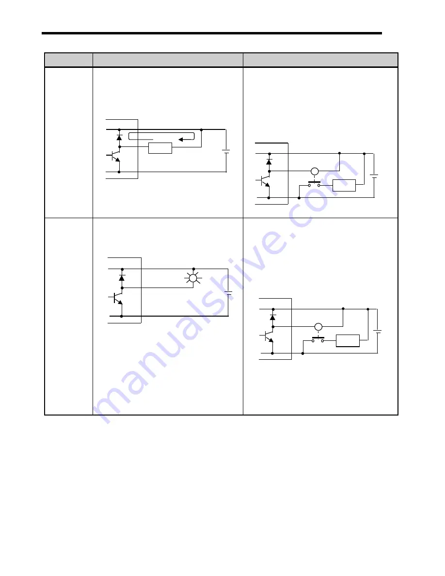
Output circuit troubles and corrective actions (continued).
Condition
Cause
Corrective actions
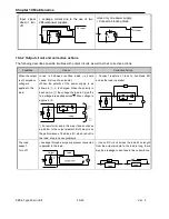
Latency in
the de-
energizing
of the
switched
output
device
The characteristics of solid state switching
devices can lead to a delayed Off time to the
inductive/resistive load.
Use an interposing relay between the
module output and the controlled load.
Consider using a transient absorbing/clamping
device across the load to lengthen the life of
the relay contacts.
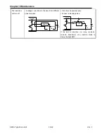
Module
output
transistor
damaged
The inrush current to the load is high enough
to permanently damage the output transistor.
Use an interposing relay between the
module output and the controlled load.
Consider using a transient absorbing/clamping
device across the load to lengthen the life of
the relay contacts
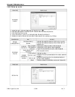
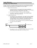
Outpu
t
Load
Output
E1
Outpu
t
Load
E
Off current
Outpu
t
Load
Summary of Contents for XBC-DN10E
Page 1: ......
Page 10: ...Table of Contents Table of Contents 6 10 10 CLEAR ALL PLC 29...


