5-6
Signals
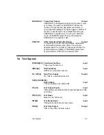
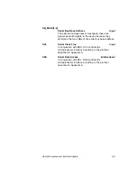
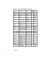
TDI[7]
Test Data Input
Input
TDI is the JTAG unit data input.
TCK[6]
Test Mode Clock
Input
TCK is the JTAG test mode clock.
5.5 Control Signals
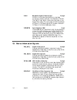
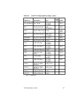
OCLK
Encoder Out/Processing Clock In
Bidirectional
OCLK is a positive-edge-triggered clock. The L64777
internally processes data based on a fraction of OCLK
(for example: scrambler, interleaver, Reed-Solomon
encoder) and references data outputs (I, Q,
FSTARTOUT) to OCLK.
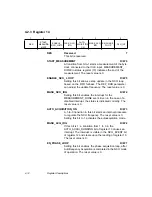
PLL_MODE[1:0]
Select PLL Mode
Input
To select the PLL mode:
0b00 or 0b01 for external PLL usage
0b11 for NCO usage
RESET_n
Reset
Input
This pin resets all internal data paths. Reset timing is
asynchronous to the device clocks. Reset affects all the
configuration registers and the filter coefficients, which
must be downloaded again after reset.
5.6 External PLL Signals
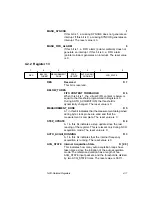
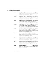
PCLK
Processing Clock: PLL Mode 2
Input
The PCLK output of the L64724 provides this clock,
which drives the digital signal processing of interpolation
and the NCO. When using Mode 1, leave this pin open.
PLL_OUT_CS PLL Current Source
3-State Output
This pin is a charge pump for an external PLL low pass
to control frequency. The comparator is frequency- and
phase-sensitive. The pin is normally on 3-state Z level
and drives positive and negative current, as required.
Depending on the configuration, the current source can
be inverted.
Summary of Contents for L64777
Page 1: ...L64777 DVB QAM Modulator Order Number I14031 A Technical Manual June 2000...
Page 10: ...x Contents...
Page 14: ...1 4 Introduction...
Page 90: ...5 10 Signals...
Page 110: ...A 8 Programming the L64777 in Serial Host Interface Mode...
Page 116: ...C 2 Monitoring Device Internal Signals...
Page 124: ......


