background image


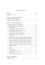
5

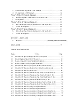
    c. 

Discriminator Alignment - (CW Method) .................................. ………..36 


    d. 

IF Amplifiers - (CW Method)......................................................………..36 


"Slave" 200 Kc. IF Channel Alignment

................................................ ………..39 

    b. 

Third IF amplifier, Adjustment of T-307 and T-308 .................. ………..39 

    c. 

IF amplifiers....................................... …………………………………...39 

"Master" 40 Kc. IF Channel Alignment

.... .........................................................40 

    b. 

40 Kc. Band-Pass Filter, Adjustment of  L-606 and L-607.......................40 

    c. 

2.5 Mc. IF Amplifier................................................................... ………..40 

"Slave" 40 Kc. IF Channel Alignment

....... .........................................................41 

    b. 

40 Kc. Band-Pass Filter, Adjustment of  L-602 and L-603........ ………..41 

    c. 

2.5 Mc. IF Amplifier................................................................... ………..41 


SECTION 5 - PARTS LIST 

    a.      Parts List...................................................................(

currently under construction


DISCLAIMER…………………………………………………………………… 75 


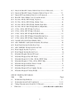
LIST OF ILLUSTRATIONS 


Figure 

Title 

         Page 

1-1      Model G-187 Special Purpose Receiver, Front View…………………….    7     

2-1      Block Diagram, Model G-187 Receiver ........................................ ………  14 


2-2      Receiver Squelch Circuit, Simplified Schematic ........................... ………  23 


2-3      Receiver COR Circuit, Simplified Schematic................................ ………  24 


4-1      Model G-187 Receiver, Top View (Dust Cover Removed)........... ………  44 


4-2      Model G-187 Receiver, Bottom View (Dust Cover Removed) .. .. ………  45 


4-3      Model G-187 Receiver, Rear View ............................................... ………  46 

4-4      Model G-187 Receiver, Panoramic Top View (Cover Removed)………...  47 

4-5      Model G-187 Receiver, Panoramic Top View Left Side (C. R.)………….  48 

4-6      Model G-187 Receiver, Panoramic Top View Right Side (C. R.)………… 49 

4-7      Model G-187 Receiver, Panoramic Bottom View (C. R.)…………………  50 

4-8      Model G-187 Receiver, Panoramic Bottom View Left Side (C. R.)………  51 

4-9      Model G-187 Receiver, Panoramic Bott. View Right Side  (C. R.)………   52 

4-10    Model G-187 Receiver, Large Component Board………………………..    54 

4-11    Model G-187 Receiver, Small Component Board……………………….     55 

4-12    Model G-187 Receiver, Auxiliary & Output Circuits (Top View)………     55 

4-13    Model G-187 Receiver, Auxiliary & Output Circuits (Bott. View)……..     55 

4-14    Model G-187 Receiver, Auxiliary & Output Circuits (Bott. View)…….      56 

Summary of Contents for G-187

Page 1: ...INSTRUCTION BOOK FOR MODEL G 187 SPECIAL PURPOSE RECEIVER LTV Electrosystems Inc A Subsidiary of Ling Temco Vought TEMCO Aerosystems Division P O Box 1056 Greenville Texas 75402...

Page 2: ...isting and unmodified LTV G 187 Receiver that has survived and upon the Instruction Manuals of some Nems Clarke units using similar components The work is dated 2010 2011 and the author is Paolo Viapp...

Page 3: ...scillator Buffer Slave Tuner Only 19 3 IF STAGES 19 a Function Switch in 200 Kc FM Position Master IF Channel 19 b Function Switch in 200 Kc AM Position Master IF Channel 20 c Function Switch in 200 K...

Page 4: ...d IF amplifier Adjustment of T 307 and T 308 32 e Third Second IF amplifier Adjustment of T 305 and T 306 32 f Second IF Amplifier Adjustment of T 303 and T 304 32 g First IF Amplifier Adjustment of T...

Page 5: ...hematic 23 2 3 Receiver COR Circuit Simplified Schematic 24 4 1 Model G 187 Receiver Top View Dust Cover Removed 44 4 2 Model G 187 Receiver Bottom View Dust Cover Removed 45 4 3 Model G 187 Receiver...

Page 6: ...om View 64 4 28 Controls in the Front Panel Bottom Side 65 4 29 AGC MON DF and Function Switches Front Panel 65 4 30 Front Panel Function Switch Rear View 65 4 31 AGC MON DF Rotary Switch rear View 66...

Page 7: ...7 Figure 1 1 Model G 187 Special Purpose Receiver Front View...

Page 8: ...trips Approx 10V RMS for 500 uV input modulated 50 at 1 Kc FM Output Stability Varies less than 2 dB for inputs above 1 uV AM Output Stability 200 kc and 40 kc strips 7 dB maximum variation for 40 dB...

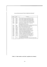
Page 9: ...9 Table 1 2 Semiconductor and Tube Complement...

Page 10: ...10 Table 1 2 Semiconductor and Tube Complement continued...

Page 11: ...hs of 200 or 40 Kc a separate high quality 600 ohm audio output a video output and a special control signal output for direction finding purposes For further details concerning the capabilities and sp...

Page 12: ...sed in their 1302 and 1502 receivers Inductuners are mechanically tuned variable inductors for VHF and UHF applications that are tuned using a common rotary shaft moving contacts along single turn or...

Page 13: ...c IF subchassis is directly fastened just to the left side panel by three 1 2 turn screws Near the rear panel of the unit are located the video audio squelch and COR circuits while the power supply ci...

Page 14: ...14 Fig 2 1 Block Diagram Model G 187 Receiver...

Page 15: ...0 Kc bandwidth only and make use of a special kind of tubes called Nuvistor in a separate subchassis that is fastened to the left side of the receiver Such a subchassis is the FM 75J 100 IF strip that...

Page 16: ...S Series placed in the rear apron of the receiver During either AM or FM operation the carrier operated relay COR is actuated by AGC voltage from the stage which functions as either a detector or seco...

Page 17: ...ble tuned over coupled band pass filter A capacity T is used to provide coupling between the primary and secondary tuned circuits The shunt element of the T is adjustable thus providing a control over...

Page 18: ...e grid circuit developing an operating bias proportional to the amplitude of the local oscillator signal This causes a minimum effect on the receiver operation due to variations in local oscillator am...

Page 19: ...on the selected mode and bandwidth a FUNCTION SWITCH IN 200 Kc FM POSITION MASTER IF CHANNEL Two high gain stages V 501 V 502 using 6DC6 tubes are followed by a 6CB6 V 503 first limiter and a 6AK5 V 5...

Page 20: ...M position and then switching to the AM 200kc position c FUNCTION SWITCH IN 200 Kc FM OR AM POSITION SLAVE IF CHANNEL Also the Slave 21 54 Mc IF channel has two high gain stages V 301 V 302 using 6DC6...

Page 21: ...etector A self resonant choke is connected in the AM output lead to prevent IF signals from leaving the IF subassembly f FUNCTION SWITCH IN 40 Kc FM OR AM POSITION SLAVE IF CHANNEL Again plate and scr...

Page 22: ...rcuit is connected in such a manner that V 103A has zero grid voltage when no signal is being received and has a negative signal applied when a carrier is being received The audio amplifier stage V 10...

Page 23: ...the V 103A plate load resistor R 129 V 103B receives only its normal cathode bias generated in its cathode bias resistor R 131 and audio signals are passed through to the output Fig 2 2 Model G 187 R...

Page 24: ...ntrol of a panel light and auxiliary equipment provided such equipment is connected to the two available sets of relay contacts through their terminating points on J 108 a socket on the chassis rear a...

Page 25: ...voltage drop across the first stage plate load resistor R 132 The connection of the second stage between 240 VDC and 150 VDC and the use of a cathode resistor R 144 biases the second stage to a level...

Page 26: ...to the carrier off position The relay has three sets of contacts two of which are made available for use in the carrier control of auxiliary equipment by their connection to J 108 on the chassis rear...

Page 27: ...ng The meter does this by reading the value of the DC component of the discriminator output a component which is zero when tuning is exact and when tuning is inexact is of a polarity determined by the...

Page 28: ...keeping in mind that Positions 1 3 AM 40 Kc or AM 200 Kc The Mon AGC rotary switch small inner knob could be in the ON AVC or the OFF MAN position in the latter case the manual RF gain control R 102...

Page 29: ...ers be disassembled and cleaned whenever they are found to be sufficiently dirty to warrant such action The overall schematic diagram contained herein will be useful in locating trouble Such trouble a...

Page 30: ...p generator lead through a small capacitor In order to avoid extraneous coupling or regeneration the sweep and the market generator leads should be dressed out and away toward the input end from the s...

Page 31: ...1 4 Mc e Discriminator Adjustment of T 508 Remove the first limiter V 503 from its socket Connect the sweep generator between pin 1 of V 504 and ground on the tube socket mounting strap nut Set the sw...

Page 32: ...tor to TP 202 on the RF chassis and ground on one of the trimmer capacitor studs Set the sweep generator output as required to produce 0 25 Volts peak scope deflection Adjust T 501 primary and T 502 s...

Page 33: ...djustment of T 301 and T 302 Reconnect the cable to J 202 Install the IF bottom cover and tighten all the mounting screws Connect the scope to first limiter grid pin 1 of V 303 Connect the sweep gener...

Page 34: ...tified by removing the 18 9 Mc oscillator and observing the pip disappear Note The adjustment of the L 602 and L 603 coils that form the 40 Kc Band Pass filter has been carefully done at the Factory a...

Page 35: ...to the extreme high frequency end until the dial is stopped by both the inductuner stops please verify this happens at the same time Hairline should align with triangle on dial if not loosen the screw...

Page 36: ...on In the event that it should become necessary to align the IF strip and a suitable sweep generator and oscilloscope are not readily available the following CW alignment procedure is included It is t...

Page 37: ...ormer T 508 remove the 6AK5 second limiter tube V 504 and note the reading of the center frequency meter M 102 If it is off center it should be centered by means of the potentiometer R 118 located on...

Page 38: ...the required bandwidth These factors suggest a rather simple alignment procedure with a minimum of equipment The resonant frequency of the primary or the secondary in the absence of the other no coupl...

Page 39: ...VTVM and connect to pin 1 control grid of V 303 Adjust T 507 and T 508 alternatively for maximum output c IF Amplifiers The characteristics of cascaded critically coupled amplifier stages are such as...

Page 40: ...mum as this will result in improper adjustment 11 Repeat steps 6 through 9 for T 302 T 303 and T 304 NOTE It is not necessary to follow this sequence as any transformer may be adjusted without affecti...

Page 41: ...tively for maximum gain Note The adjustment of the L 602 and L 603 coils that form the 40 Kc Band Pass filter has been carefully done at the Factory and no further attempt should normally be required...

Page 42: ...Gnd V 204 6AK5 N A Gnd 6 3 VAC N A N A N A N A MAIN CHASSIS V 101 12AU7A 135 Gnd 6 7 Gnd Gnd 137 0 1 6 8 6 2 AC V 102 12AU7A 235 138 141 Gnd Gnd 235 138 141 6 2 AC V 103 12AU7A 145 0 27 24 Gnd Gnd 210...

Page 43: ...A N A Gnd 200 Kc IF AMPLIFIER Slave Channel Function Switch in 200 Kc AM Position V 301 6DC6 N A N A 6 3 AC Gnd N A N A Gnd V 302 6DC6 N A N A 6 3 AC Gnd N A N A Gnd V 303 6CB6 N A N A 6 3 AC Gnd N A...

Page 44: ...44 Fig 4 1 Model G 187 Receiver Top View Cover Removed...

Page 45: ...45 Fig 4 2 Model G 187 Receiver Bottom View Covers Removed...

Page 46: ...46 Fig 4 3 Model G 187 Receiver Rear View...

Page 47: ...47 Fig 4 4 Model G 187 Receiver Panoramic Top View Cover Removed...

Page 48: ...48 Fig 4 5 Model G 187 Receiver Panoramic Top View Left Side Cover Removed...

Page 49: ...49 Fig 4 6 Model G 187 Receiver Panoramic Top View Right Side Cover Removed...

Page 50: ...50 Fig 4 7 Model G 187 Receiver Panoramic Bottom View Covers Removed...

Page 51: ...51 Fig 4 8 Model G 187 Receiver Panoramic Bottom View Left Side Covers Removed...

Page 52: ...52 Fig 4 9 Model G 187 Receiver Panoramic Bottom View Right Side Covers Removed...

Page 53: ...53 Table 4 2 Model G 187 Receiver Component Boards Lists...

Page 54: ...54 Fig 4 10 Model G 187 Receiver Large Component Board...

Page 55: ...55 Fig 4 11 Model G 187 Receiver Small Component Board Fig 4 12 Model G 187 Receiver Auxiliary Output Circuits Top View Fig 4 13 Model G 187 Receiver Auxiliary Output Circuits Bottom View...

Page 56: ...56 Fig 4 14 Model G 187 Receiver Master Slave RF Tuners Top View...

Page 57: ...57 Fig 4 15 Model G 187 Receiver Master Slave Tuners Bottom View Covers Removed...

Page 58: ...58 Fig 4 16 Model G 187 Receiver Master Slave Tuners Panoramic Bottom View Covers Removed...

Page 59: ...59 Fig 4 17 Model G 187 Receiver Master RF Tuner Bottom View Cover Removed...

Page 60: ...60 Fig 4 18 Model G 187 Receiver Slave RF Tuner Bottom View Cover Removed...

Page 61: ...61 Fig 4 19 Model G 187 Receiver 21 4 Mc 200 Kc BW IF Strip Master Slave Channels Top View Fig 4 20 Model G 187 Receiver 21 4 Mc 200 Kc BW IF Strip Bottom View C R...

Page 62: ...ig 4 21 Model G 187 Receiver 21 4 Mc 200 Kc BW IF Strip Master Slave Channels Bottom View Input Side Fig 4 22 Model G 187 Receiver 21 4 Mc 200 Kc BW IF Strip Master Slave Channels Bottom View Output S...

Page 63: ...or Strip Master Slave Channels Top View Fig 4 24 Model G 187 Receiver 2 5 Mc 40 Kc BW IF Nuvistor Strip CEI Label on the chassis side Fig 4 25 Model G 187 Receiver 2 5 Mc 40 Kc BW IF Nuvistor Strip Ma...

Page 64: ...64 Fig 4 26 Model G 187 Receiver 2 5 Mc 40 Kc BW IF Nuvistor Strip Master Channel Bottom View Fig 4 27 Model G 187 Receiver 2 5 Mc 40 Kc BW IF Nuvistor Strip Slave Channel Bottom View...

Page 65: ...Model G 187 Receiver Controls in the Front Panel Bottom Side Fig 4 29 Model G 187 Receiver AGC MON DF and Function Switches in the Front Panel Fig 4 30 Model G 187 Receiver Rear of the Front Panel Fun...

Page 66: ...66 Fig 4 31 Model G 187 Receiver Rear of the AGC MON DF Rotary Switch Fig 4 32 Model G 187 Receiver The Power Supply Section Top View Fig 4 33 Model G 187 Receiver The Power Supply Section Bottom View...

Page 67: ...67 Fig 5 1 Model G 187 Receiver Schematic Diagram Master RF Tuner...

Page 68: ...68 Fig 5 2 Model G 187 Receiver Schematic Diagram Slave RF Tuner...

Page 69: ...69 Fig 5 3 Model G 187 Receiver Schematic Diagram 21 4 Mc 200 Kc BW IF Strip Master and Slave Channels...

Page 70: ...70 Fig 5 4 Model G 187 Receiver Schematic Diagram 2 5 Mc 40 Kc BW IF Nuvistor Strip Master and Slave Channels...

Page 71: ...71 Fig 5 5 Model G 187 Receiver Schematic Diagram Main Chassis Circuits...

Page 72: ...72 Fig 5 6 Model G 187 Receiver Schematic Diagram Mainframe...

Page 73: ...73 Fig 5 7 Model G 187 Receiver Schematic Diagram Power Supply Circuits...

Page 74: ...74 Fig 5 8 Model G 187 Receiver Schematic Diagram Various Details...

Page 75: ...s free for private use and you are allowed to redistribute it freely subject to the following restrictions 1 The origin of this manual must not be misrepresented and you must not claim that you wrote...

Reviews: