363-206-295
Circuit Pack Descriptions
Issue 1
December 1997
7-21
Clock Output Functions
7
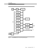
Intra-shelf Timing Distribution.
7
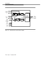
The generated timing signals are distributed
through output drivers to the main and function unit slots. The TG circuit pack
provides eight differential 51.84-MHz master clock signals and eight differential
8-kHz composite STS-1 frame sync signals. In the 8-kHz sync signal, every fourth
pulse is stretched to double width, providing an embedded 2-kHz reference for the
virtual tributary (VT) superframe synchronization.
DS1 Outputs .
7
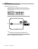
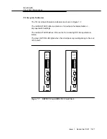
The DS1 output port can be provisioned by hardware switches for
MULT mode or DS1 timing synchronization (SYNC OUT) mode.
■
SYNC OUT Mode
— The DS1 output port of the BBF2B TGS circuit pack can be
provisioned to be a derived DS1 signal traceable to a received
optical line used for network timing distribution. The SYNC OUT
capability is available for a DDM-2000 set for external-timing or line-
timing.
■
MULT Mode
— The DS1 output port of the TGS circuit pack can be provisioned to
output a buffered copy (at a DSX level) of the DS1 signal at the input
port. A DS1 traceable source is applied to the first DDM-2000 shelf.
The output of the first shelf is then cabled to the second shelf, and
all subsequent shelves fed from the previous ones. In this way, a
MULT chain is formed from a single DS1 reference. The MULT
capability is only available for a DDM-2000 provisioned for external-
timing.
Protection Circuitry
7
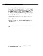
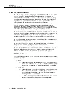
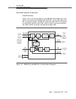
In both external and line (formerly loop)-timing modes, the synchronization
references are continuously monitored for error-free operation. If the active
reference becomes corrupted, the TG circuit pack will select the standby
reference without causing service degradations (that is, hitless reference
switching). If both reference inputs are corrupted, the TG circuit pack enters
holdover mode where the DPLL holds the on-board oscillator frequency at the last
good reference sample while the references are repaired.
In addition, optional 1x1 nonrevertive TG circuit pack protection is provided. When
the active TG circuit pack microcontroller determines that its clock output is out of
tolerance, it suppresses its timing outputs and signals its TG circuit pack
companion unit of its failed condition. The suppressed timing outputs cause a
timing hardware switch to the standby TG circuit pack by the transmission circuit
packs.

