363-206-295
Circuit Pack Descriptions
7-42
Issue 1
December 1997
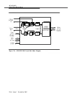
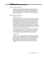
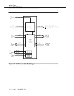
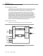
Figure 7-17. BBG12 3STS1E Circuit Pack Block Diagram
Timing Circuitry
7
The BBG12 3STS1E circuit pack derives its timing information from the recovered
clock of the incoming EC-1 signals. In the transmit direction, a 51.84 MHz clock is
recovered from the incoming EC-1 signal and is used to recover EC-1 data. In the
receive direction, the 3STS1E circuit pack receives its timing from the working and
standby TSI circuit packs. The 3STS1E circuit pack selects between the supplied
timing signals as requested by the SYSCTL circuit pack via the intra-shelf control
bus.
Protection Circuitry
7
Optional 1x1 nonrevertive BBG12 3STS1E circuit pack protection is provided.
Switch points for the STS-1 side of the BBG12 3STS1E are located on the TSI
circuit packs. Switch points for the EC-1 side are implemented with relays on the
3STS1E circuit pack. To ensure that the relays can be operated when the circuit
pack fails, the relay is controlled by the SYSCTL via the control interfaces. Also, if
power to the board is lost, the relay switches autonomously to the standby state.
When a new board is inserted, it defaults to the standby state until provisioned
active by the SYSCTL.
Driver
Loopback
EC-1
Receiver
LBO
Protection
Hybrid
Relays
Intrashelf
3 STS-1
-48V A
-48V B
Timing
Control
To/From
To/From
STSX-1
To/From
From
From
Shelf
-48V Fuses
To/From
SYSCTL
(Service &
Protection)
(Service &
Protection)
TSI CPs
TSI CPs
Companion
CP
STS-1
Byte
Processing
STS-1
Pointer
Processor
EC-1
3 EC-1s

