3
3
MACOM Technology Solutions Inc. (MACOM) and its affiliates reserve the right to make changes to the product(s) or information contained herein without notice.
Visit
for additional data sheets and product information.
For further information and support please visit:
DC
-
0026091
3
MAAL-011207-QR3000
Rev. V4
Low Noise Amplifier
0.15 - 6 GHz
Biasing Options
The MAAL
-
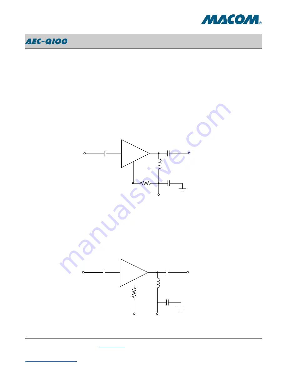
011207 bias can be set in 2 different ways: using only V
DD
or using separate V
DD
and V
BIAS
voltages.
A separate V
BIAS
voltage allows pin 5 (V
BIAS
) to be used as an enable pin to power the device up and
down during operation.
For both bias methods select the value of R
BIAS
to achieve the desired current based on the tables on page 4, and
use DC blocks at pin 2 (RF
IN
) and pin 7 (RF
OUT
/ V
DD
).
DC Block
RF
OUT
RF
IN
V
DD
DC Block
R
BIAS
RF Choke
Bypass
2
7
5
Biasing Option
-
Separate V
DD
and V
BIAS
Voltages (V
BIAS
≤
V
DD
)
To use separate V
DD
and V
BIAS
voltages, connect pin 7 (RF
OUT
/ V
DD
) to V
DD
through an RF choke inductor and
connect pin 5 (V
BIAS
) to V
BIAS
through bias resistor R
BIAS
as shown in Figure 2. Typical current (I
BIAS
) draw for pin 5
(V
BIAS
)
is 1.4 mA @ V
BIAS
= 3 V and 1 µA @ V
BIAS
= 0 V.
Typical current (I
DD
) draw for pin 7 (RF
OUT
/ V
DD
) is
< 1 µA @ V
BIAS
= 0 V.
Biasing Option
-
V
DD
only
To use only V
DD
, connect pin 7 (RF
OUT
/ V
DD
) to V
DD
through an RF choke inductor and connect pin 5 (V
BIAS
) to V
DD
through bias resistor R
BIAS
as shown in Figure 1.
Figure 1
Figure 2
DC Block
RF
OUT
RF
IN
V
DD
DC Block
R
BIAS
RF Choke
Bypass
V
BIAS
2
7
5


