V1.4
– Apr-13
User’s Manual
Page 15 of 34
NOTE
: Care must be taken to implement an orderly shut-down sequence along
with supplying power for a certain period of time after initiating the shut-down
sequence. Abrupt removal or drop of power while the module is running has
risks ranging from minor impact on TTFF to fatal corruption of flash memory
code area (Please refer to
“Power ONOFF Sequences and Power-On-Reset
(POR) on A2100-AB Application
Notes”)!
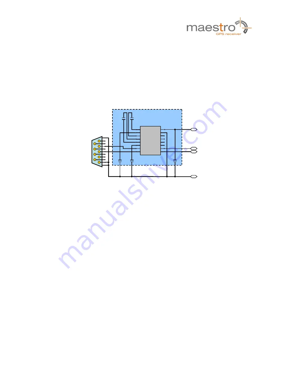
For completeness the following pictures show the use of an RS232 level shifter.
GND
1
2
3
4
5
6
7
8
9
C1
0
.1
µ
F
C2
0
.1
µ
F
C3
0
.1
µ
F
C4
0
.1
µ
F
C5
0
.1
µ
F
RS232 Level Shifter
RS232 Out
D
B
9
f
e
m
a
le
3.3V
Vcc
GND
T1O
R1I
R1O
T1I
T2I
R2O
C1+
V+
C1-
C2+
C2-
V-
T2O
R2I
MAX3232
Tx
Rx
GND
1
2
3
4
5
6
7
8
9
C1
0
.1
µ
F
C2
0
.1
µ
F
C3
0
.1
µ
F
C4
0
.1
µ
F
C5
0
.1
µ
F
RS232 Level Shifter
RS232 Out
D
B
9
f
e
m
a
le
3.3V
Vcc
GND
T1O
R1I
R1O
T1I
T2I
R2O
C1+
V+
C1-
C2+
C2-
V-
T2O
R2I
MAX3232
Tx
Rx
Figure 6: RS232 level shifter for minimum configurations
Remarks:
Place C1 to C5 (here: 0.1µF) close to MAX3232. For capacity values see
datasheet of actual component used.
Use 3.3V level shifter (MAX3232 or equivalent).


