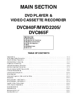
SERVICE MANUAL
Main Section
I
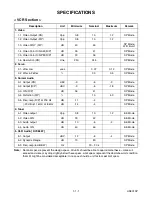
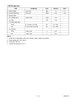
Specifications
I
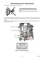
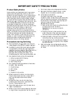
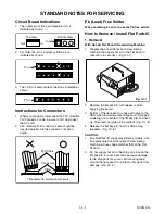
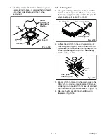
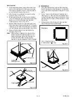
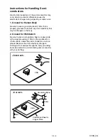
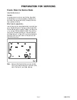
Preparation for Servicing
I
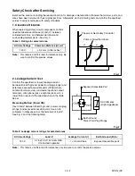
Adjustment Procedures
I
Schematic Diagrams
I
CBA’s
I
Exploded Views
I
Parts List
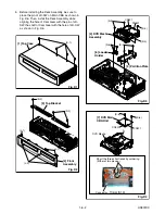
When servicing the deck
mechanism, refer to MK14 Deck
Mechanism Section.
Deck Mechanism Part No.:
N2440FL, N2460FL
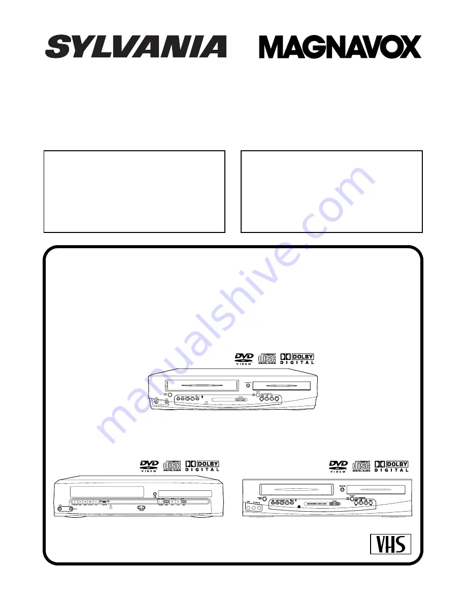
DVD PLAYER &
VIDEO CASSETTE RECORDER
DVC840F
MWD2205
DVC865F
Summary of Contents for sylvania mwd2205
Page 16: ...1 6 3 H9801DC Fig D5 S 7 S 7 S 7 S 8 8 VCR Chassis Unit...
Page 41: ...1 12 10 H9802SCM8 Main 8 8 Schematic Diagram VCR Section DVC865F...
Page 63: ...1 18 2 H9801PEX Packing S2 S2 S2 S2 S1 Unit A14 S3 X1 X4 X20 X5 X2 X3...
Page 71: ...DVC840F MWD2205 DVC865F H9801UD H98K0UD H9802UD 2005 01 28...