background image

2-9

2-10

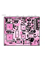
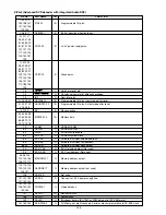
MAIN BOTTOM VIEW

IC701
IC700
IC500

IC550

IC614

IC606

TR490

IC605

IC602

TR491

IC490

IC603

IC600

IC850

TR600

IC801
IC800

TR117

IC300

IC803

TR167

IC901

IC802

TR112

TR170 ~TR712

IC991
IC110

IC971
IC951
IC931

IC911

TR111
TR110

TR114

IC852

IC703

IC851

IC201

IC100

TR125

Summary of Contents for DV7000

Page 1: ...E O TABLE OF CONTENTS SECTION PAGE 1 MAIN UNIT 1 1 TECHNICAL SPECIFICATIONS 1 1 1 2 CONNECTION FACILITIES 1 2 1 3 INFORMATIONS 1 3 1 4 SERVICING HINT 1 4 1 5 DISASSEMBLY 1 5 1 6 REPLACEMENT OF PRINCIPAL COMPONENTS 1 6 1 7 SERVICE MODE 1 8 1 8 ELECTRICAL ADJUSTMENT 1 10 1 9 WAVEFORM 1 12 1 10 WIRING DIAGRAM 1 13 1 11 BLOCK DIAGRAM 1 15 1 12 SCHEMATIC DIAGRAM 1 17 1 13 PARTS LOCATION 1 27 1 14 EXPLO...

Page 2: ...L PHILIP DA AMAZONIA IND ELET ITDA CENTRO DE INFORMACOES AO CEP 04698 970 SAO PAULO SP BRAZIL PHONE 0800 123123 Discagem Direta Gratuita FAX 55 11 534 8988 JAPAN Technical MARANTZ JAPAN INC 35 1 7 CHOME SAGAMIONO SAGAMIHARA SHI KANAGAWA JAPAN 228 8505 PHONE 81 42 748 1013 FAX 81 42 741 9190 EUROPE TRADING MARANTZ EUROPE B V P O BOX 80002 BUILDING SFF2 5600 JB EINDHOVEN THE NETHERLANDS PHONE 31 40 ...

Page 3: ...ms 330 ohms RCA pin Jack x 2 system Digital audio output Optical output Optical connector x 1 Coaxial output 0 5 Vp p 75 ohm RCA pin Jack x 1 DVD Iinear audio characteristics Frequency response 4 Hz 22 kHz Fs 48 kHz 4 Hz 44 kHz Fs 96 kHz S N ratio More than 110 dB Fs 48 kHz 24 bit PCM Dynamic range More than 100 dB Fs 48 kHz 24 bit PCM Total harmonic distortion Less than 0 0025 Fs 48 kHz 24 bit PC...

Page 4: ...t 0 4V into 75 Ohm CVBS S Video Pin 16 fast switching in 0 4V into 75 Ohm CVBS S Video 1 3 into 75 Ohm RGB 1 3 into 75 Ohm RGB Pin 17 GND Pin 17 GND Pin 18 GND Pin 18 GND Pin 19 CVBS Y out 1Vpp 0 1V 1 Pin 19 CVBS Y out 1Vpp 0 1V 1 Pin 20 CVBS Y in 1Vpp 0 1V 1 Pin 20 CVBS Y in 1Vpp 0 1V 1 Pin 21 GND Pin 21 GND 1 100 White 2 Burst Level 3 color bar chroma level 75 What are regional codes Motion pict...

Page 5: ...select the subtitle language that you want to read Soundtrack language DVDs are recorded with up to 8 different soundtrack languages If a disc has more than one language you can select the soundtrack language that you want to listen to Multi angles On some DVDs scenes have been filmed from different angles up to a maximum of 9 On these discs you can select the angle that you want to watch Please r...

Page 6: ...rs SBC444 Disc with DO errors black spots and fingerprints SBC444A 4822 397 30245 Disc 65 min 1kHz without no pause 4822 397 30155 Max diameter disc 58 0 mm 4822 397 60141 Torx screwdrivers Set straight 4822 395 50145 Set square 4822 395 50132 13th order filter 4822 395 30204 DVD test disc PAL 4822 397 10131 SERVICE HINTS ...

Page 7: ...ve 6 screws and remove the top cover 3 Remove a top right side screw on the power supply PCB and remove the GND lug wire 4 Remove 3 connectors of the wire harness from or to front panel assembly 5 Remove 2 screws of left and right side of the front panel assembly 6 Remove the front panel assembly 7 Remove the retainer on the DVD mechanism 8 Remove FFC and wire harness from the DVD main PCB which m...

Page 8: ...s Fig 6 2 A SCREW 6 REPLACEMENT OF PRINCIPAL COMPONENTS 6 1 2 Removal of the TRAVERSE MECHA 1 Remove the four b screws on the MAIN PCB and then disconnect the P800 connector on the MAIN PCB Fig 6 3 2 Short the laser diode protection circuit on the PICK UP BLOCKÕs flexible cable with solder as shown Caution To protect the laser diode from damage caused by high voltage static electricity a laser dio...

Page 9: ...cting the P200 connector on the MECHANISM PCB 6 2 Replacement of the SPINDLE MOTOR Because the SPINDLE MOTOR position is very critical jitter adjustment should be performed after replacement 1 Disconnect the P300 connector on the MECHANISM PCB 2 Insert a Philips type screw driver into the hole on the TURN TABLE of the SPINDLE MOTOR and remove the two screws 6 3 Replacement of the PICK UP BLOCK Rep...

Page 10: ... 0 The status will be in REMOTE CONTROL TEST MODE and FLD shows RC6 000000 10 If press some button on the remote controller FLD shows a code of that pressed button 11 Press the NEXT button again then the version number of the main microprocessor IC600 on the DVD main PCB will be shown on the FLD 12 Press the NEXT button again then the version number of the slave microprocessor QF01 on the front PC...

Page 11: ...r a couple of seconds 3 Type versions can be changed by pressing button and button 4 Memorize the version by pressing PLAY button 5 The FL display shows VERIFY OK after a couple of seconds 6 Power OFF the mains switch DISPLAY VERSIONS USA U1B U1G N1B N1G HK S PORE S1G CHINA K1B K1G J APAN F1B F1N NO REGION Incorrect setup EUROPE VERSIONS DISPLAY F1B F1N E2P ALL JPN U1B U1G E2P ALL USA N1B N1G E2P ...

Page 12: ... side one layer and press the F F button repeatedly until the pickup block reaches almost the center position of its movable range 2 Set the oscilloscope to the DC input mode and connect it to the TP201 HOT and the TP102 D GND on the MAIN PCB 3 Adjust the VR202 so that the DC level is minimum The DC level should be less than 1 8 V 8 3 CD TRACKING BALANCE 1 Set the VR110 at its center position prio...

Page 13: ...P107 5 Press the button again Then the DVD laser will light ON and the FL display shows E3 00 6 Press the button again Then the CD laser will light ON and the FL display shows E3 01 7 Adjust the voltage at the test point TP120 by VR121 that the value must be same as TP107 10mV value measured on 4 process 8 Press the button twice of time Then the DVD laser will light ON and the FL display shows E3 ...

Page 14: ...equirements Refer the circuit diagram page 1 25 and 1 26 100V AC 120V AV 220V AC 1 2 3 4 1 2 3 4 1 2 3 4 50V 5µsec 50V 5µsec 100V 5µsec 10V 5µsec 10V 5µsec 10V 5µsec 5V 5µsec 5V 5µsec 5V 5µsec 0 1V 5µsec 0 1V 5µsec 0 1V 5µsec ...

Page 15: ...1 13 1 14 1 10 WARNINGS ...

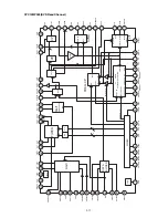
Page 16: ...1 15 1 16 1 11 BLOCK DIAGRAM ...

Page 17: ...1 17 1 18 1 12 SCHEMATIC DIAGRAM AND PARTS LOCATION ...

Page 18: ...1 19 1 20 ...

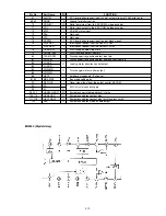
Page 19: ...Audio L R Output to RF Modulator 9 VOUT_RF Video CVBS Output to RF Modulator 10 GNDV3 Video Switches Ground 3 11 FILTER Chroma Trap Filter 12 VCCV3 Video Switches Supply 3 8V 13 NC Not Connected 14 GNDV2 Video Switches Ground 2 15 NC Not Connected 16 VCCV2 Video Switches Supply 2 8V 17 FBOUT_TV Fast Blanking Output to TV Scart 18 FBIN_VCR see Note 1 Fast Blanking Input from VCR Scart 19 FBIN_ENC F...

Page 20: ...1 23 1 24 TIME TRACK TRACK TITLE TOTAL CHAPTER FTS SCAN PBC TRACK VCD CHAPTER SHUFFLE REPEAT TITLE A B ...

Page 21: ...1 25 1 26 ...

Page 22: ...F11 QF01 QF04 QF06 QF07 QF05 QF10 QF09 QF03 QF02 QF12 PP01 QP18 QP19 QP20 QP22 QP02 QP01 QP25 QP24 QP04 QP12 QP14 QP13 QP13 QP11 QP09 QP08 QP06 QP05 QP07 QP10 QP03 PK01 QK01 QK04 QK06 QK03 QK05 PS01 PL01 1 13 PARTS LOCATION ...

Page 23: ...QS02 QS01 QS03 QS05 QS07 QV10 QV05 QV08 QV15 QV12 QH02 QH12 Even number QH03 QH11 Odd number QS14 QS12 QS11 QS13 QS15 QS18 QV04 QV11 QV14 QV18 QS51 QS50 QS52 QV03 QV02 QV07 QV06 QV09 QV10 QV16 QV13 QV17 QV18 QS08 QS09 ...

Page 24: ...OLD 284T154240 045B BLACK 9965 000 01975 BUTTON POWER BLACK 255W270010 045B GOLD 9965 000 01395 BUTTON POWER GOLD 255W270110 050B BLACK 9965 000 05026 ESCUTCHEON TRAY FRONT BLK 383K063010 050B GOLD 9965 000 05027 ESCUTCHEON TRAY FRONT GLD 383K063110 051B BLACK 9965 000 05028 DVD BADGE BLK 386K251030 051B GOLD 9965 000 05029 DVD BADGE GLD 386K251130 009G 9965 000 05030 LEG GOLD HOT STAMP F 383K0570...

Page 25: ...L 0 0 2 L 0 0 5 N K ONL Y 5 1 1 0 3 x 6 M 0 3 4 G F C 0 1 T P 0 1 PV0 1 0 3 1 G x 2 PS0 1 5 4 0 5 3 M L 0 0 1 5 1 1 0 3 x 6 M L 0 0 3 N O N L Y L 0 0 4 5 1 1 0 3 x 8 M 0 5 0 B 0 5 1 B 5 1 2 8 3 x 8 M 0 0 1 A 0 2 0 G 0 2 1 G 5 1 2 8 3 X 8 M 5 1 2 8 3 X 8 M 0 5 6 G 0 2 6 G 0 0 1 Z MARK MAT ERI AL F I N I S H M ST E EL COPPER U ST E EL BL ACK SY MBOL ST Y L E PA RT S NA ME 5 1 1 0 B H M S CREW 5 1 2 ...

Page 26: ... 4822 126 11703 CER CHIP 0 01µF DK98103300 C871 N 4822 126 11703 CER CHIP 0 01µF DK98103300 C876 N 4822 126 13883 CER CHIP 220pF 5 CG 50V DD95221300 C881 N 4822 126 13883 CER CHIP 220pF 5 CG 50V DD95221300 C884 N 4822 126 11687 CER CHIP 0 1µF DK98104200 C887 N 4822 126 11687 CER CHIP 0 1µF DK98104200 C951 N 4822 124 90354 ELECT 100µF M 16V RA 2 OA10701620 C953 N 4822 124 80067 ELECT 4 7µF M 50V RA...

Page 27: ...10 R988 N 4822 051 30103 CHIP 10kΩ 5 1 16W NN05103610 R989 N 4822 051 30222 CHIP 2 2kΩ 5 1 16W NN05222610 R990 N 4822 051 30103 CHIP 10kΩ 5 1 16W NN05103610 PE01 SEMICONDUCTORS D801 N 4822 130 83715 CHIP DIODE 1SS301 DAN202U HZ21005000 D802 N 4822 130 80346 CHIP DIODE 02CZ8 2 HZ30004050 D803 N 4822 130 80346 CHIP DIODE 02CZ8 2 HZ30004050 D805 N 4822 130 80346 CHIP DIODE 02CZ8 2 HZ30004050 D807 N 4...

Page 28: ... 051 30102 CHIP 1kΩ 5 1 16W NN05102610 RF41 4822 117 12925 CHIP 47kΩ 5 1 16W NN05473610 RF42 4822 051 30101 CHIP 100Ω 5 1 16W NN05101610 RF43 4822 051 30101 CHIP 100Ω 5 1 16W NN05101610 RF46 RF49 4822 051 30101 CHIP 100Ω 5 1 16W NN05101610 RF50 4822 116 83829 CHIP 270Ω 5 1 16W NN05271610 RF51 4822 051 30103 CHIP 10kΩ 5 1 16W NN05103610 RF52 4822 051 30152 CHIP 1 5kΩ 5 1 16W NN05152610 RF53 4822 05...

Page 29: ... 10V RA 2 OA22701020 CP26 4822 124 41539 ELECT 47µF M 16V RA 2 OA47601620 CP27 4822 124 90351 ELECT 0 1 µF M 50V RA 2 OA10405020 CP28 4822 124 90353 ELECT 100µF M 10V RA 2 OA10701020 CP29 N 4822 124 90353 ELECT 100µF M 10V RA 2 OA10701020 CP30 4822 124 22276 ELECT 47µF M 50V RA 2 OA47605020 CP31 4822 124 22276 ELECT 47µF M 50V RA 2 OA47605020 CP32 9965 000 01318 ELECT 220µF M 10V RA 2 OA22701020 C...

Page 30: ...211 10K 10K BA20001000 QP09 4822 130 11604 TRS 2SB1020 HT21020100 QP10 4822 130 60588 DIG TRS DTC114ES UN4211 10K 10K BA20001000 QP11 N 4822 209 80655 IC NJM78M08 8V 0 5A HC38508090 QP12 4822 130 61227 DIG TRS DTA114ES UN4111 10K 10K BA10001000 QP13 4822 130 62548 TRS 2SB1185 E F HT211852B0 QP14 4822 130 42715 TRS 2SA1048 2SA933S 2SA1267 ETC HT10001000 QP18 4822 130 41947 TRS 2SC2458 2SC1740S HT30...

Page 31: ...T 470µF M 10V RA 2 OA47701020 CV14 4822 126 11703 CER CHIP 0 01µF DK98103300 CV15 4822 126 13689 CER CHIP 18pF DD95180300 CV16 4822 126 11663 CER CHIP 12pF 5 CG 50V DD95120300 CV17 9965 000 04997 CER CHIP 5pF 0 25pF CH DD90050300 CV18 4822 122 33782 CER CHIP 56pF DD95560300 CV19 9965 000 04997 CER CHIP 5pF DD90050300 CV20 4822 122 33777 CER CHIP 47pF 5 CG 50V DD95470300 CV21 4822 124 41539 ELECT 4...

Page 32: ... 051 30471 CHIP 470Ω 5 1 16W NN05471610 RS25 4822 116 90503 CHIP 150Ω 5 1 10W NI05151110 RS28 RS29 4822 051 30222 CHIP 2 2kΩ 5 1 16W NN05222610 RS32 RS33 4822 117 12891 CHIP 220kΩ 5 1 16W NN05224610 RS34 4822 117 12891 CHIP 220kΩ 5 1 16W NN05224610 RS35 4822 051 30223 CHIP 22kΩ 5 1 16W NN05223610 RS36 4822 051 30223 CHIP 22kΩ 5 1 16W NN05223610 RS37 4822 051 30101 CHIP 100Ω 5 1 16W NN05101610 RS38...

Page 33: ... QH04 4822 130 61425 CHIP TRS 2SC2873 Y HX328731B0 QH05 4822 130 42839 F E T 2SK369 BL VDGS 40V PDO 4W HF203691B0 QH06 4822 130 42839 F E T 2SK369 BL VDGS 40V PDO 4W HF203691B0 QH07 4822 130 63928 CHIP TRS 2SA1312 B HX113121B0 QH10 QH11 4822 130 63929 CHIP TRS 2SC3324 B HX333241B0 QH12 4822 130 63929 CHIP TRS 2SC3324 B HX333241B0 QS01 4822 130 61906 DIG TRS DTC114EU BA20035210 QS02 4822 130 61903 ...

Page 34: ...007 JACK 24FLT SM1 TB JST YJ07021200 JV04 4822 265 10678 TERMINAL YKF51 5506 YT02011010 JV05 F K S U TERMINAL 3P RCA PIN JACK YKC21 4010 YT02030580 JV07 N 9965 000 04999 JACK FFC 23FMN BTRA ST YJ07019470 JV08 9965 000 05008 TERMINAL 2P RCA JACK YKC21 3926 YT02021590 LS01 4822 142 60422 PULSE TRANSF TPS247MN 0386AN TP41042030 LV01 9965 000 00458 CHOKE COIL 8 2µH EL0405 LC18223900 LV02 4822 157 6044...

Page 35: ... VIEW AND PARTS LIST 2 28 2 4 ELECTRICAL PARTS LIST 2 30 IMPORTANT NOTICE This service manual explains the product DV7000 which mounted the DVD module TKM1000MZ with the main board C3M1 only Products which mounted C3M1 has product serial number MZ01XXXXXXXXXX All other products have mounted M3C1 main board Product serial number MZ00XXXXXXXXXX Spare parts for M3C1 main board are not available In ca...

Page 36: ......

Page 37: ...2 1 2 2 Not for DV4000 2 1 SCHEMATIC DIAGRAM AND PARTS LOCATION ...

Page 38: ...2 3 2 4 ...

Page 39: ...2 5 2 6 Not for DV4000 ...

Page 40: ...2 7 2 8 MAIN TOP VIEW IC111 TR113 TR100 TR106 TR120 TR115 IC122 IC121 TR804 TR806 TR300 TR200 IC311 IC120 TR190 TR201 TR202 IC202 IC203 TR802 TR801 IC607 IC507 IC610 IC613 IC503 IC501 IC702 TR500 IC502 ...

Page 41: ...00 IC500 IC550 IC614 IC606 TR490 IC605 IC602 TR491 IC490 IC603 IC600 IC850 TR600 IC801 IC800 TR117 IC300 IC803 TR167 IC901 IC802 TR112 TR170 TR712 IC991 IC110 IC971 IC951 IC931 IC911 TR111 TR110 TR114 IC852 IC703 IC851 IC201 IC100 TR125 ...

Page 42: ...2 11 2 12 ...

Page 43: ...2 13 2 14 MECHA TOP VIEW MECHA BOTTOM VIEW TR90 TR37 TR34 TR33 IC1 TR1 TR35 TR36 IC2 IC4 TR32 IC3 TR31 MT100 LOADING ...

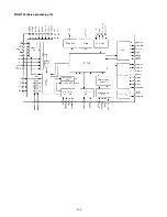
Page 44: ...C11AP000 DVD Pre AMP 67 85 86 87 88 93 94 95 96 97 98 99 89 90 91 92 100 68 66 1 2 AVSS LPCVREF LPCI1 LPCI2 LPCO LDON VFE2N4 FBAL VGAOUT FE3XINP VFEI P FEO VFEI N FE3XINN VFE1N3 ASI ASO AVSS TPSP TPSO TPSN REFCAPFIX REFCAPDLY CLIMITER AVSS AVDD AVDD 10k POF NEG POF HOLD LIMIT TBAL VDOWN VREF VUP AVSS TE CMN TE N CMOUT CMP AVDD VREF POF 2 2 POFP OFTR 2 POFN AVSS XDVD XCD2 XCD4 OFTR OFTRVTH BUF COFT...

Page 45: ...EQ CP JIT SYNK CP PD 51 52 1 2 3 4 DATA SLICER 5 6 7 8 9 10 11 12 13 14 15 16 17 18 19 20 21 22 CAP5 23 ADJDSRFD 24 VSS RDCK VCO IN VCO ON U D OUT RFCP DLY SRD VDD 25 26 27 28 PDWIN 29 VCOIN 30 PLFLT 31 VSS VDD FCPO 32 33 34 RPCP 35 VDD DSRF MUX EXT SD SLDTIN BF2 BF1 VBF2 VBF1 8X DIFF TO SINGLE CONVERTER TW 2 36 37 38 39 40 41 42 43 VL2 D A D A 44 VL1 VOUT 45 46 VO2 47 VO1 48 LZ3V VSS RIREF2 AGC C...

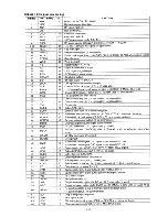
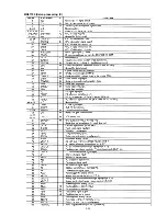
Page 46: ...FSO control output L 48 kHz H 44 1 kHz 31 SYSRST O System reset output 32 DRPOUT I Drop out input 33 63 91 119 Vss Ð Ground pin 34 C Ð Capacitor connecting pin 35 PAL NTSC O Video decoder PAL NTSC select output 36 ENRST O Video encoder IC reset output 37 XDARST O DAC reset output 38 DVcc Ð 5 V power supply pin for digital circuit 39 DVss Ð Ground pin for digital circuit 40 FCSBAL I Focus balance a...

Page 47: ... I Disc tray open detect input pin 79 CLOSE SW I Disc tray close detect input pin 80 CLAMP SW I Disc changer tray position detect input pin 81 PHOT IN I Disc changer tray position detect photo sensor input pin 82 LOAD F O Loading motor direction control output 83 LOAD R 84 CHG M R O Disc changer motor control output 85 CHG M L 86 HSTX I hardware standby pin Pulled up 87 89 MD0 MD2 I Bus mode setti...

Page 48: ...2 20 MN66261 CD signal processing ...

Page 49: ...2 21 MN66261 CD signal processing ...

Page 50: ...2 22 MN67700 Servo processing IC ...

Page 51: ...2 23 MN67700 Servo processing IC ...

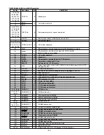
Page 52: ... changed on the falling edge of PLLCLK 37 SDTIO I O Serial bit data I O 38 ASPSCK O 296ns clock 27 MHz 8 output 39 SEN O High enable CPU to write data to 8 read channel registers 40 PLLOK O DVD frame sync H O K 41 LDON O Turn on the Laser diode 42 XDVD O DVD mode control output 43 XCD2 O 2X CD mode control output 44 XCD4 O 4X CD mode control output 47 51 54 56 SRMDT0 7 I O SRAM data bus 57 61 64 7...

Page 53: ... state control 168 XHSTCS O Decipher chip select 176 STENABLE I Stream data request 177 181 STD0 7 O Output stream data bus 185 187 183 GENCLK I 27 MHz clock input 188 STCLK O Output stream data transfer clock falling edge active 6 75 MHz 189 STVALID O Output stream data valid 190 XVCS O Latched video decoder chip select 191 XVDS O CPU read write strobe 192 HRXW O CPU write strobe XWEH 193 ASCK O ...

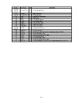
Page 54: ... 15 I O Memory data 66 68 70 72 73 74 76 78 79 LDQM O SDRAM LDQM 80 UDQM O SDRAM UDQM 82 MWE O SDRAM write enable 84 SD CLK O SDRAM system clock 85 SD CAS O Active low SDRAM column address 86 SD RAS O Active low SDRAM row address 88 90 SDCS0 1 O Active low SDRAM bank select 92 EDO CAS O EDO column address Not used 94 EDO RAS O EDO row address Not used 96 98 100 102 104 106 MADDR0 11 O Memory addre...

Page 55: ... data from DVD DSP or CDG 4 7 CDG SDATA VSFY S0S1 SCLK signal input 191 VREQUEST O Video request Decoder asserts VREQUEST to indicate that the video input buffer has available space 192 VSTROBE I Video strobe signal input 194 AREQUEST O Audio request Decoder asserts AREQUEST to indicate that the audio input buffer has available space 196 V DACK I Video data acknowledge in synchronous mode Asserted...

Page 56: ...2 28 2 3 EXPLODED VIEW AND PARTS LIST TKM1000MZ ...

Page 57: ... BT BID30X08STL CMT nsp 15 9965 000 04602 DISC TRAY 294W163010 16 9965 000 04603 HOLDER TRAVERSE 294W104010 17 9965 000 04604 INSULATOR 294W130010 18 9965 000 04605 SP PUSH HOOK 294W115010 19 9965 000 04606 HOOK L S 294W258010 20 9965 000 04607 SHAFT SCREW PART 294W117010 21 nsp PAN17X3 5STL CMT PS3 nsp 22 9965 000 04608 SP PUSH L S SP000980R 23 9965 000 04609 SW MICRO MPU10420MLB0 SM000330R 24 ns...
Page 58: ...capacitor One way type Mylar 10 50V 7 Capacity value Examples 7 Capacity value 0 001 F 1000 pF 102 0 1 F 104 0 0018 F 182 0 56 F 564 0 01 F 103 1 F 105 0 015 F 153 1 The above CODES R R C C and C are omitted on the schematic diagram in some case 2 On the occasion be confirmed the common parts on the parts list 3 Refer to Common Parts List for the other common parts Rl05 DD4 DK4 NOTE NOTE ON SAFETY...

Page 59: ...IC931 9965 000 04649 IC PCM1735E 2K HC105400R IC951 9965 000 04649 IC PCM1735E 2K HC105400R IC971 9965 000 04649 IC PCM1735E 2K HC105400R IC991 9965 000 04650 IC TC74HC4053AFTEL HC105360R TRANSISTORS TR100 9965 000 04651 UMG4N BA21711000 TR101 9965 000 04651 UMG4N BA21711000 TR102 9965 000 04651 UMG4N BA21711000 TR103 9965 000 04651 UMG4N BA21711000 TR104 9965 000 04651 UMG4N BA21711000 TR105 9965...

Reviews: