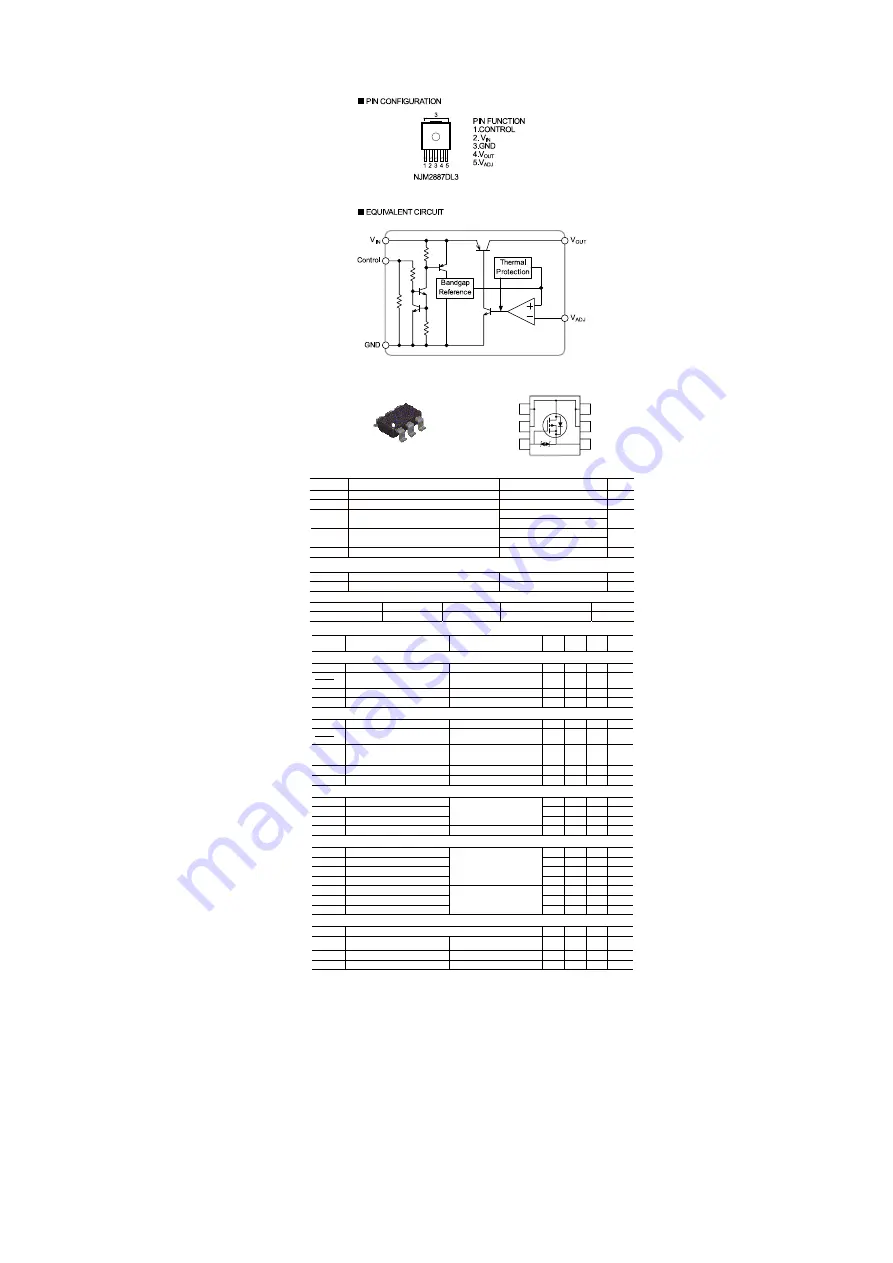
NJM2887_E (FRONT : IC81)
FDC608PZ (DIGITAL : Q203)
D
D
D
S
D
G
SuperSOT -6
TM
Absolute Maximum Ratings
T
A
=25
o
C unless otherwise noted
s
ti
n
U
s
g
n
it
a
R
r
e
t
e
m
a
r
a
P
l
o
b
m
y
S
V
DSS
V
0
2
–
e
g
a
tl
o
V
e
c
r
u
o
S
-
n
i
a
r
D
V
GSS
Gate-Source Voltage
±
12
V
Drain Current – Continuous
(Note 1a)
–5.8
I
D
0
2
–
d
e
s
l
u
P
–
A
Maximum Power Dissipation
(Note 1a)
1.6
P
D
(Note 1b)
0.8
W
T
J
, T
STG
Operating and Storage Junction Temperature Range
–55 to +150
°
C
Thermal Characteristics
R
θ
JA
Thermal Resistance, Junction-to-Ambient
(Note 1a)
78
°
C/W
R
θ
JC
Thermal Resistance, Junction-to-Case
(Note 1)
30
°
C/W
Package Marking and Ordering Information
Device Marking
Device
Reel Size
Tape width
Quantity
s
ti
n
u
0
0
0
3
m
m
8
’
’
7
Z
P
8
0
6
C
D
F
Z
8
0
6
.
6
5
4
1
2
3
Electrical Characteristics
T
A
= 25°C unless otherwise noted
Symbol
Parameter
Test Conditions
Min Typ Max Units
Off Characteristics
BV
DSS
Drain–Source Breakdown Voltage
V
GS
= 0 V, I
D
= –250
µ
A
–20
V
∆
BV
DSS
∆
T
J
Breakdown Voltage Temperature
Coefficient
I
D
= –250
µ
A,Referenced to 25
°
C
–10
mV/
°
C
I
DSS
Zero Gate Voltage Drain Current
V
DS
= –16 V, V
GS
= 0 V
–1
µ
A
I
GSS
Gate–Body Leakage
V
GS
=
±
12 V, V
DS
= 0 V
±
10
µ
A
On Characteristics
(Note 2)
V
GS(th)
Gate Threshold Voltage
V
DS
= V
GS
, I
D
= –250
µ
A
–0.4
–1.0
–1.5
V
∆
V
GS(th)
∆
T
J
Gate Threshold Voltage
Temperature Coefficient
I
D
= –250
µ
A,Referenced to 25
°
C
3
mV/
°
C
R
DS(on)
Static Drain–Source
On–Resistance
V
GS
= –4.5V, I
D
= –5.8 A
V
GS
= –2.5V, I
D
= –5.0 A
V
GS
= –4.5V,I
D
= –5.8A,T
J
=125
°
C
26
38
35
30
43
m
Ω
I
D(on)
On–State Drain Current
V
GS
= –4.5 V, V
DS
= –5 V
–20
A
g
FS
Forward Transconductance
V
DS
= –10 V,
I
D
= –5.8 A
22
S
Dynamic Characteristics
C
iss
F
p
0
3
3
1
e
c
n
a
ti
c
a
p
a
C
t
u
p
n
I
C
oss
F
p
0
7
2
e
c
n
a
ti
c
a
p
a
C
t
u
p
t
u
O
C
rss
Reverse Transfer Capacitance
V
DS
= –10 V,
V
GS
= 0 V,
f = 1.0 MHz
230
pF
R
G
Gate Resistance
V
GS
= 15 mV, f = 1.0 MHz
12
Ω
Switching Characteristics
(Note 2)
t
d(on)
s
n
4
2
3
1
e
m
i
T
y
a
l
e
D
n
O
–
n
r
u
T
t
r
s
n
6
1
8
e
m
i
T
e
s
i
R
n
O
–
n
r
u
T
t
d(off)
s
n
5
4
1
1
9
e
m
i
T
y
a
l
e
D
f
f
O
–
n
r
u
T
t
f
Turn–Off Fall Time
V
DD
= –10 V,
I
D
= –1 A,
V
GS
= –4.5 V, R
GEN
= 6
Ω
60
96
ns
Q
g
C
n
3
2
7
1
e
g
r
a
h
C
e
t
a
G
l
a
t
o
T
Q
gs
C
n
3
e
g
r
a
h
C
e
c
r
u
o
S
–
e
t
a
G
Q
gd
Gate–Drain Charge
V
DS
= –10 V,
I
D
= –5.8 A,
V
GS
= –4.5 V
6
nC
Drain–Source Diode Characteristics and Maximum Ratings
I
S
Maximum Continuous Drain–Source Diode Forward Current
–1.3
A
V
SD
Drain–Source Diode Forward
Voltage
V
GS
= 0 V, I
S
= –1.3 A
(Note 2)
–0.7
–1.2
V
t
rr
Diode Reverse Recovery Time
I
F
= –5.8 A, d
iF
/d
t
= 100A/µs
40
60
ns
Q
rr
Diode Reverse Recovery Charge
I
F
= –5.8 A, d
iF
/d
t
= 100A/µs
15
23
nC
Notes:
1.
R
θ
JA
is the sum of the junction-to-case and case-to-ambient resistance where the case thermal reference is defined as the solder mounting surface of the drain
pins. R
θ
JC
is guaranteed by design while R
θ
CA
is determined by the user's board design.
a. 78°C/W when mounted on a 1in
2
pad of 2oz copper on FR-4 board.
b. 156°C/W when mounted on a minimum pad.
2.
Pulse Test: Pulse Width
≤
300
µ
s, Duty Cycle
≤
2.0%
79


