DISASSEMBLY
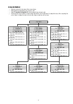
• Remove each part in the order of the arrows below.
• Reassemble removed parts in the reverse order.
• Read
"Precautions During Work"
before reassembling removed parts.
• If wire bundles are removed or moved during adjustment or part replacement, reshape the wires after completing the
work. Failure to shape the wires correctly may cause problems such as noise.
FRONT PANEL ASSY
See "
DISASSEMBLY
"
1. FRONT PANEL ASSY
and "
EXPLODED VIEW
"
HEADPHONE&SETUP MIC PCB
(Ref. No. of EXPLODED VIEW : 09)
F-HDMI PCB
(Ref. No. of EXPLODED VIEW : 12)
FRONT PCB
(Ref. No. of EXPLODED VIEW : 14)
BT PCB
(Ref. No. of EXPLODED VIEW : 42)
USB PCB
(Ref. No. of EXPLODED VIEW : 51)
TOP COVER
POWER TRANS
See "
DISASSEMBLY
"
7. POWER TRANS
and "
EXPLODED VIEW
"
POWER TRANS
(Ref. No. of EXPLODED VIEW : 31)
RADIATOR ASSY
See "
DISASSEMBLY
"
2. RADIATOR ASSY
and "
EXPLODED VIEW
"
GUIDE CENTER FRONT PCB
(Ref. No. of EXPLODED VIEW : 15)
GUIDE CENTER PCB
(Ref. No. of EXPLODED VIEW : 16)
GUIDE PCB(L)
(Ref. No. of EXPLODED VIEW : 18)
AMP PCB
(Ref. No. of EXPLODED VIEW : 24)
GUIDE BT
(Ref. No. of EXPLODED VIEW : 48)
HDMI PCB
See "
DISASSEMBLY
"
4. HDMI PCB
and "
EXPLODED VIEW
"
HDMI PCB ASSY
(Ref. No. of EXPLODED VIEW : 47)
CX870 MODULE ASSY
(Ref. No. of EXPLODED VIEW : 60)
CX870 MIDDLE ASSY
(Ref. No. of EXPLODED VIEW : 61)
AV PCB
See "
DISASSEMBLY
"
5. AV PCB
and "
EXPLODED VIEW
"
FRONT_CNT PCB
(Ref. No. of EXPLODED VIEW : 43)
SIDE_CNT PCB
(Ref. No. of EXPLODED VIEW : 46)
AUDIO_VIDEO PCB
(Ref. No. of EXPLODED VIEW : 45)
SPK PCB
See "
DISASSEMBLY
"
6. SPK PCB
and "
EXPLODED VIEW
"
SPEAKER PCB
(Ref. No. of EXPLODED VIEW : 38)
SMPS PCB
See "
DISASSEMBLY
"
8. SMPS PCB
and "
EXPLODED VIEW
"
SMPS PCB
(Ref. No. of EXPLODED VIEW : 37)
REG ASSY
See "
DISASSEMBLY
"
3. REG ASSY
and "
EXPLODED VIEW
"
REG_CNT PCB
(Ref. No. of EXPLODED VIEW : 39)
REG PCB
(Ref. No. of EXPLODED VIEW : 40)
11
Summary of Contents for NR1605/FB
Page 8: ...Personal notes 8 ...
Page 26: ...Personal notes 26 ...
Page 103: ...CX870 7P 8P 5P PLATE PLATE 2P 7P 4P 7P 11P 5P 8P PLATE S30SC6MT WIRING DIAGRAM 103 ...
Page 140: ...Personal notes Personal notes 140 ...
Page 161: ...2 FL DISPLAY FLD 018BT021GINK FRONT U4400 PIN CONNECTION GRID ASSIGNMENT q T7 161 ...
Page 162: ...ANODE CONNECTION 162 ...


